The best solution for AR glasses? Integrating Micro LEDs with advanced CMOS
- author:
- 2023-03-25 09:16:27
Recently, SOREN STEUDEL and MICLEDI MICRODISPLAYS released a paper stating that bonding a 300 mm silicon-based GaN LED wafer to a CMOS backplane of the same size is the best method to produce Micro LED displays with a pitch of only a few microns. The highlights are as follows:
Currently, Micro LEDs used for large displays face challenges related to this huge transfer and repair of defective chips, and large-scale production is hindered. Nowadays, when Micro LEDs are used in micro display applications such as AR glasses, they also face a series of new problems.
According to reports, one way to make Micro LED display modules is to integrate Micro LEDs and CMOS-ASIC backplanes to control and drive Micro LEDs through the latter. This approach eliminated the problems associated with massive transfers, but encountered a series of other obstacles.
For example, in terms of usage scenarios, AR glasses require brightness of more than 1Mnits, pixel spacing of less than 3m, resolution of more than 2K, ultra-low power consumption and acceptable cost. These need to be implemented in a lightweight module.
As of now, existing micro-display manufacturing methods cannot meet all these specifications. To this end, SOREN STEUDEL and MICLEDI MICRODISPLAYS say they are developing a method needed to achieve high-volume, low-cost manufacturing.

Although the level of miniaturization is very attractive, it is difficult to achieve; because even manufacturing full HD displays with a spacing of 5 m will approach the retina size limit of the exposure tool, which will affect manufacturability and yield.
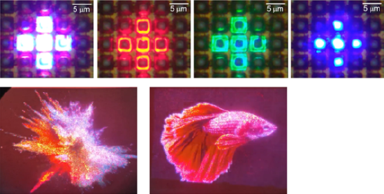
According to the manufacturing yield model in the paper (as shown in the figure below), assuming that red, green and blue Micro LEDs are integrated side by side, even if the target resolution is reduced to only 40 pixels per degree, a spacing of less than 3 m is required to exceed the yield of 50%.

Alternatively, by independently manufacturing emitters of three different colors and then integrating them with the optical combiner, some conditions can be significantly relaxed. This is closer to the yield model of existing color display technology called sequential liquid crystal displays on silicon.
In terms of integration solutions, die-to-wafer transfer is used, which is to create red, green and blue emitter arrays by transferring and placing one pixel at a time, or by gluing the entire array into a single chiplet. In this way, the spacing can be reduced to 10mmm with a fixed yield loss.
Currently, the related production process of stacked silicon wafers has been put into use, combining sequential 3D structures with through-substrate holes and wafer-to-wafer hybrid bonding. The latter is typically used to produce back-illuminated imagers with pitches as small as 3 m and is used in R & D departments to combine 300 mm wafers with pitches of less than 1 m with coverings of less than 200 nm.
Through the integrated solution, they achieved a record aperture of up to 65%, or 2.5 m in a hexagonal pitch configuration of 3 m. Our current approach is to use an optical combiner to combine the output of red, green and blue chips. On red LEDs, they are also working to improve efficiency and color point. By enhancing light output coupling in the top corners that are useful for waveguide integration and suppressing light emission outside this angle, brightness can be improved by a factor of 2 - 4.
TAG:
Guess you want to see it
Popular information
-
JBD officially released AR glasses with LED micro-display FOV optical waveguide solution
-
The best solution for AR glasses? Integrating Micro LEDs with advanced CMOS
-
3.15 Gala XR technology attracted attention! XR gradually becomes the "standard" for parties

-
Sony Virtual Production Studio opens! XR shooting of tall buildings is gradually emerging
-
Innovative design of LED digital virtual shooting mobile control system
the charts
- Sony Virtual Production Studio opens! XR shooting of tall buildings is gradually emerging
- 3.15 Gala XR technology attracted attention! XR gradually becomes the "standard" for parties
- The best solution for AR glasses? Integrating Micro LEDs with advanced CMOS
- Innovative design of LED digital virtual shooting mobile control system
- JBD officially released AR glasses with LED micro-display FOV optical waveguide solution