Sharp: Self-luminescent quantum LEDs to realize the next generation of displays
- author:
- 2024-06-05 16:42:31
Quantum dots (QD) have attracted great interest as a new material for display applications. Luminescent quantum dots are semiconductor particles of nanometer size that generally exhibit narrow emission spectra and high internal quantum efficiency. These unique characteristics enable quantum dots to produce a wide color gamut (WCG) and low power consumption when used in displays. With this in mind, Sharp expects the technical application of QD materials on displays to develop in three main steps (Figure 1)). The first step began in 2013 with QD backlights for liquid crystal displays (LCDs), in which QD sheets are used as wavelength conversion materials to achieve pure RGB white light. The second step is to use a direct pixel color conversion method starting from 2022 to convert the blue light wavelength of each pixel in the display into green and red wavelengths. This was mainly developed in conjunction with organic light emitting diode (oled) displays, known as QD-OLED displays. The final step is the current-injection quantum dot self-emission method (hereinafter referred to as nanoLED, a light-emitting diode structure created from nanoparticles), which is expected to become the next generation of displays to replace OLED displays.

Figure 1. Evolution steps of quantum dot (QD) displays
The technology before step 2 has been put into practical use, while the technology from step 3 is still in the R & D stage. As strong candidates for the next generation of displays, we focus on nanoLEDs, where red, green and blue (RGB) light-emitting layers are patterned directly through photolithography. In this article, we describe the potential applications of nanoLEDs from the perspective of technology and market demand. We also discussed the latest developments and challenges in implementing nanoLEDs.
Fit between technology and market demand
Most display methods that have attracted attention as state-of-the-art technologies limit the availability of products due to manufacturing limitations, such as the ability to manufacture very tiny pixels with high efficiency, very high brightness displays, and glass-based processes that require the use of large motherboards. Lower unit costs (Table 1).
table 1. Compatibility of technology with market needs. *

* Green bar indicates the applicable product range
OLED is the only self-luminous display that has widely penetrated the market. They are recognized for their high contrast, thinness and compatibility with flexible substrates that are more suitable for self-emissive displays. OLEDs are roughly divided into two technologies based on their coloring methods. The first method is to pattern the RGB emissive layer directly onto each subpixel, where each emissive layer is formed by deposition using a fine metal mask (FMM) or RGB-OLED. Another approach is to combine a white OLED layer and a color filter technology (WOLED). Instead of patterning the light-emitting layer of each RGB subpixel, a WOLED layer is formed as a common layer and a color filter is formed for each subpixel to achieve colorization.
RGB-OLED is the most widely used technology. Since RGB direct patterning has less energy loss, RGB-OLED is mainly used in wearable devices, smartphones, tablets and notebook computers, among which low-power performance is very important. However, due to the size and resolution limitations of FMM, RGB-OLED cannot be easily applied to TVs that require large screens or augmented and virtual reality (AR/VR) devices that require ultra-high resolution. WOLED is suitable for this situation.
The configurations of these displays vary. WOLEDs for large displays are driven by thin film transistor (TFT) backplane substrates composed of indium gallium zinc oxide (IGZO), while ultra-high resolution WOLEDs are driven by silicon complementary metal oxide semiconductor (CMOS) TFT substrates. In addition, the OLED element configuration used to emit white light is different between the two methods. Depending on the coloring method, both large and medium size and high resolution OLEDs are defined as the same WOLED in this paper.
LCDs with QD backlights are mainly used in televisions and displays. QD backlights contribute to a huge improvement in color purity. In addition, in recent years, the combination of QD and Miniled backlights has reduced the overall thickness of the display, so it has also been used in some notebook computers and tablet computers. MiniLED backlights contain thousands of blue LEDs with a size of hundreds of microns. By individually controlling the brightness of these blue LEDs, contrast can be greatly improved, which has long been considered a weakness of LCDs. In addition, when used in conjunction with QD sheets, this method is superior to traditional LCDs in expanding the color gamut. Due to these advantages, it is expected to be widely used in notebooks and tablets in the near future.
QD-OLED TVs and displays will be launched to the market in 2022. Their WCG and wide viewing angle performance have been well received and further applications are expected. However, its application may be limited to products with large screen size, and there is no further progress. Current QD-OLED methods require a relatively thick QD layer of about 10 m to effectively absorb the light emitted by the blue OLED layer and convert it to green and red. The QD color conversion layer is individually patterned for each red and green subpixel by inkjet, but due to the accuracy of inkjet patterning, the current resolution of QD-OLED is limited to ~200 ppi. In addition to the low power efficiency of blue OLEDs, QD-OLEDs also suffer energy losses from the QD color conversion layer, so energy efficiency is still an opportunity for improvement.
NanoLEDs, sometimes referred to as electroluminescent quantum dots (QD-EL) or QD-LED, are expected to be the next generation of technology that can achieve excellent performance (high brightness, WCG and high contrast) for displays. The manufacturing method will determine the product coverage of nanoLEDs. Several methods have been proposed to fabricate nanoLEDs based on QD patterning technology (Figure 2).

Figure 2. Schematic diagram of the patterning methods being considered for NanoLED displays
Inkjet printing is a major deposition process in which ink from quantum dots is dispensed to target locations. The required ink drop size can be minimized, thereby reducing the cost of the QD ink. This method has strong advantages. There have been many demonstrations of nanoLED patterns using inkjet printing, but there are some problems with high-resolution patterns. Therefore, the application of inkjet printed nanoLEDs will be limited to televisions and displays, similar to QD-OLEDs, where QDs are patterned in the same way as color conversion layers.
Lithography is also a promising technique for high-resolution QD patterning based on two methods. One uses a photoresist material, which reacts with ultraviolet light to form an insoluble matrix; the other is called a lift-off method, which first patterns the photoresist, deposits quantum dots, and then uses the quantum dots to remove the photoresist pattern. Both methods have been used in nanoLEDs. Manufacturing nanoLEDs through photolithography is more difficult than inkjet printing because QDs can be damaged during the process. However, if a process technology based on lithography can be established, it will have significant advantages. Lithography is the most widely used method for manufacturing electronic devices, including LCDs, and is expected to be suitable for applications ranging from high-resolution small displays to large displays, similar to LCDs, with no technical limitations.
Promote the development of NanoLED displays
Recently, advances in materials and process technology have enabled multiple display manufacturers to develop active-matrix (AM) nanoLED displays. TCL has launched a 32-inch AM hybrid display that uses red and green NanoLEDs combined with blue OLEDs. BOE showcased a 55-inch AM display with RGB nanoLEDs. Samsung Display uses RGB nanoLEDs composed of cadmium-free (Cd) QDs to make a 6.95-inch AM display. Although cadmium-containing quantum dots show excellent luminescent properties, their toxicity has been considered to have adverse effects on the environment. The successful development of displays using cadmium-free quantum dots will be a major achievement in the practical application of nano-LEDs. These additive-manufactured displays are manufactured using inkjet printing technology.
There are few reports of using lithography to develop AM nanoLED displays, which is technically challenging. Recently, Sharp reported the successful fabrication of a 6.2-inch cadmium-free quantum dot AM nanoLED display using photolithography technology (Figure 3). This product demonstrates the practicality of ultra-high resolution, which is one of the characteristics of lithography technology. Figure 4 shows the experimental results of high-resolution patterning of nanoLEDs using a passive matrix test unit on a Si wafer. Despite having an ultra-high resolution of 3,994 ppi, crosstalk was observed when RGB emission. This is the highest resolution self-luminous device created by drawing red, green and blue separately.

Figure 3. Full-color image display of a 6.2-inch cadmium-free nanoLED patterned by photolithography
TAG:
Guess you want to see it
Popular information
-
Analysis of Sony Micro OLED high-brightness technology
-
Jichuang North's OLED driver chips are mass-produced, and all supply chains are localized
-
Sharp: Self-luminescent quantum LEDs to realize the next generation of displays
-
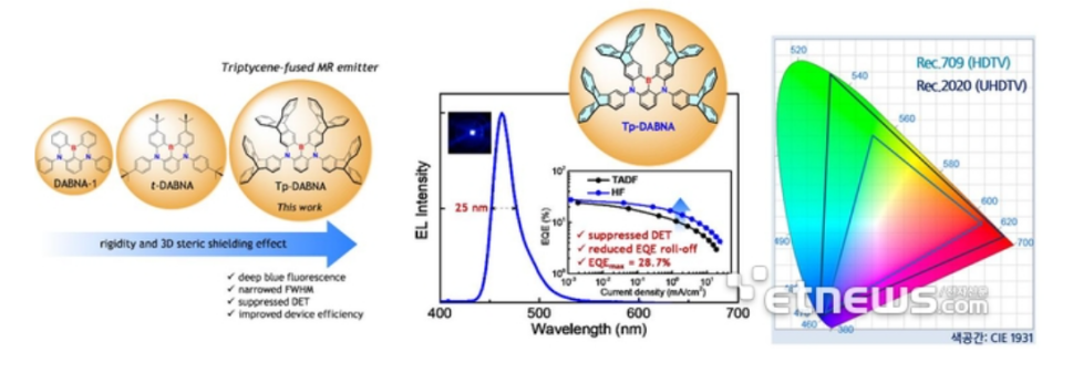
Inha University's blue OLED luminous efficiency sets a new record, reaching 29%
-
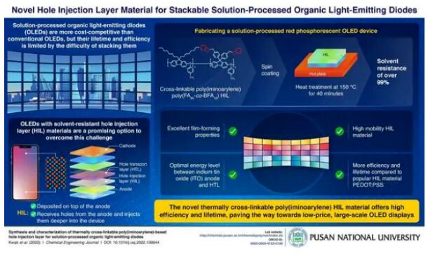
Busan National University develops a more economical solution for OLED panels
-
The industry's first AMOLED under-screen directional sounding technology comes out
the charts
- Jichuang North's OLED driver chips are mass-produced, and all supply chains are localized
- Busan National University develops a more economical solution for OLED panels
- The industry's first AMOLED under-screen directional sounding technology comes out
- Inha University's blue OLED luminous efficiency sets a new record, reaching 29%
- Analysis of Sony Micro OLED high-brightness technology
- Sharp: Self-luminescent quantum LEDs to realize the next generation of displays