Micro-LED is new, and the core technology needs to be targeted?
- author:
- 2024-05-27 10:01:52
From shelving black technology to becoming one of the best technologies such as international giants Samsung, Sony, and most LED display companies, the development of Micro-LED has achieved a qualitative leap. Why has the commercialization process of Micro-LED not achieved a large-scale explosion despite the simultaneous promotion of many factories? What are the thorny and important development issues behind this? How is the solution progressing?
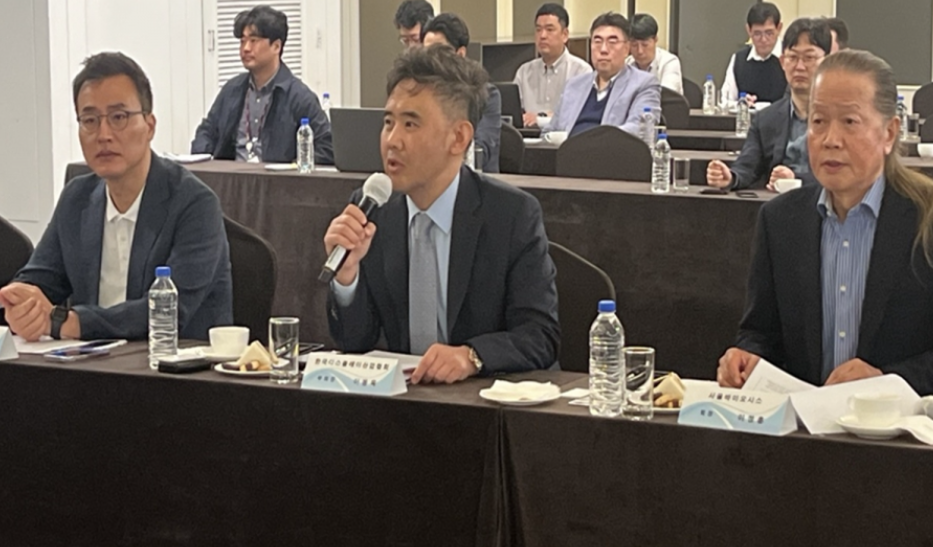
On April 17, Chenxian Optoelectronics released a number of TFT-based Micro-LED splicing products at InfoComm China 2024. In just two years, Chenxian Optoelectronics has achieved the leap from frequent introduction of Micro-LEDs to production lines. This rapid development speed has attracted widespread attention in the industry. 
In this issue, Display Home will take a deep look at Chenxian Optoelectronics to see which core technologies they have focused on and overcome, thereby achieving Micro-LED acceleration.
01
InfoComm launches new, Chen Xian attracts industry attention again
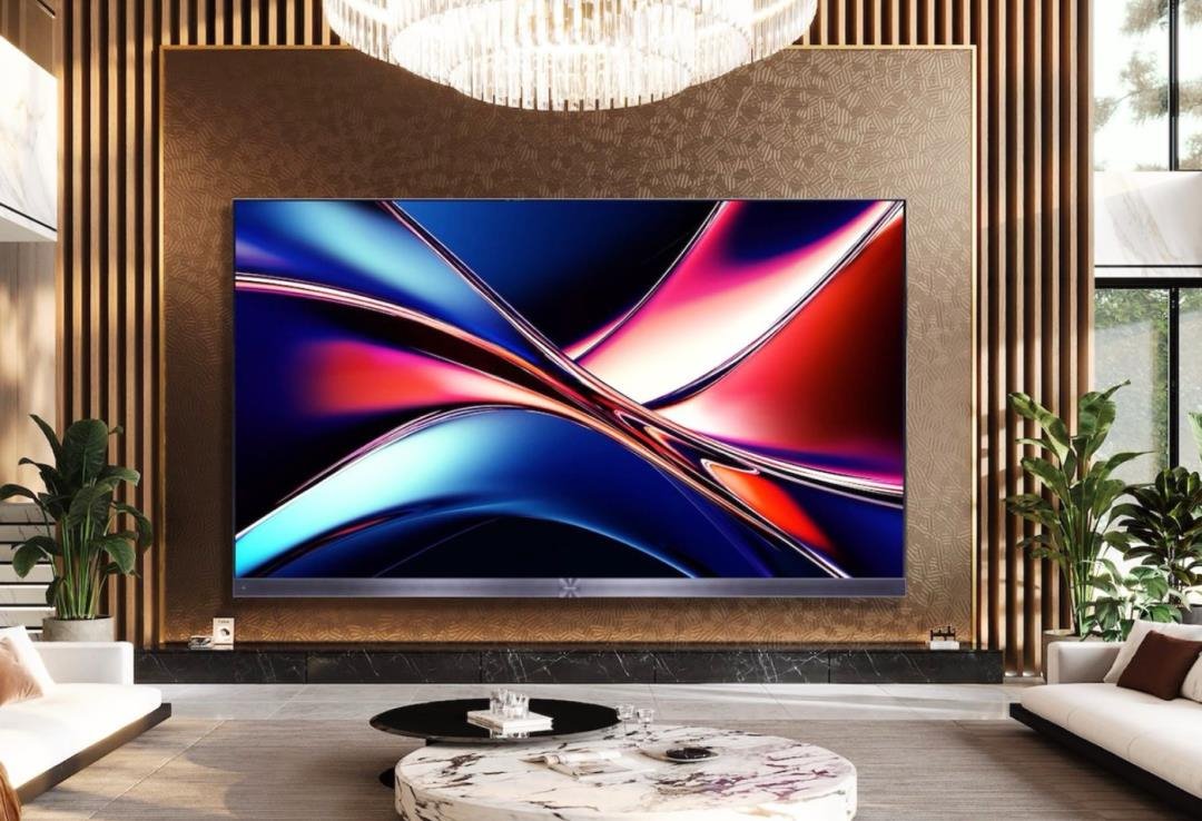
InfoComm China 2024, Chenxian Optoelectronics will release the first 14.5-inch P0.5 TFT-based Micro-LED splicing box, 27-inch TFT-based P0.7 Micro-LED splicing box, and its world's first 108-inch P0.7 TFT-based Micro-LED splicing screen in China.
Chenxian Optoelectronics InfoComm2024 Live Display
According to Display Home's summary of Chenxian Optoelectronics's new products, the dot spacing is as small as 0.5 and 0.7 mm. It mainly uses 25-micron LED chips and is equipped with the country's first Micro-LED dedicated driver IC to achieve 10 bits and seam less than 20 microns, etc.; and these characteristics are closely related to massive transfer, TFT backplane, and driver IC technologies.
02
Problems in the commercialization of Micro-LED
Let's first take a look at the current technical difficulties visible in the commercialization of Micro-LEDs.
From an industrial macro perspective, Micro-LEDs are currently facing a series of challenges such as accuracy, yield, efficiency and cost when they enter large-scale commercialization.
In order to achieve high-performance Micro-LED displays, unprecedented manufacturing precision is needed, which makes traditional manufacturing techniques no longer applicable. With the continuous development of new technologies, iterative upgrades of processes have become inevitable, but this has also brought about problems in yield and efficiency, further increasing the cost of all aspects of production, thus restricting the large-scale industrialization of Micro-LED technology.
Specifically, the three most critical technical problems at present include massive transfer, TFT backplane manufacturing and driving technology. Whether these problems can be solved will directly affect the commercialization and market penetration of Micro-LED technology.
■ Difficulty 1: Huge transfer
Massive transfer refers to a technology that transfers Micro-LED chips grown on epitaxial substrates to target substrates at high speed and precision. It is the key to restricting the mass production of Micro-LEDs. Therefore, whoever can master this key technology first will have the opportunity to quickly seize the future display market.
Take a 4K resolution Micro-LED display panel as an example. There are about 8.3 million pixels on it, and each pixel consists of three LED chips representing three colors: red, green, and blue (RGB). This means that there are nearly 25 million Micro-LED chips on a 4K display panel, which requires LED chip transfer equipment to meet both high efficiency and high yield standards to meet mass production needs.
At present, the more mainstream massive transfer methods are seal transfer technology, laser transfer technology, or a combination of these two technologies.
■ Difficulty 2: TFT backplane manufacturing
From the perspective of Micro-LED's core integration process and massive transfer technology, TFT backplates using flat panel display technology not only have advantages in surface flatness compared with traditional PCB circuits, but also can better undertake massive transfer processes; However, this technology still faces many challenges and problems in practical application and production processes.
First, in terms of manufacturing costs, manufacturing TFT backplates requires high-precision equipment and processes, which usually include but are not limited to lithography machines, chemical vapor deposition (CVD) systems, physical vapor deposition (PVD) systems, etchers, and cleaning and inspection equipment. These advanced equipment require high acquisition and maintenance costs, which to some extent leads to high initial investment and production costs.
Secondly, the practical application of technology. When TFT backplates are used to splice into large displays, the technical challenges faced are particularly significant.
In particular, the realization of sidewall routing technology and thick copper connection technology is the key to ensuring the performance and reliability of large-screen displays. During the design stage and manufacturing process, engineers must cleverly arrange the circuit layout and connection methods on the TFT backplane, while also ensuring that the overall flatness and stability of the glass substrate are not affected.
To achieve this goal, a range of sophisticated engineering techniques and materials science knowledge is involved. For example, sidewall routing technology requires circuit lines to be able to transition smoothly at the edge of the substrate while maintaining signal integrity and low resistance. Thick copper technology involves depositing a thicker layer of copper on the substrate to provide better conductivity and thermal management, but this may affect the flatness of the substrate.
These technical problems put forward higher requirements for production yield and cost control.
■ Difficulty 3: Driving architecture
Since the light-emitting characteristics of LED chips are different from those of LCDs and oleds, the existing driving architecture cannot be directly used to realize Micro-LED displays. Limited by the light emitting characteristics of the current small size LED chips, the analog driving method will bring problems such as gray scale cannot be expanded and power consumption is too high. In contrast, digital driving can use a fixed large driving current and adjust the display brightness through different display durations. Only by combining the two can a driving architecture suitable for Micro-LED displays be developed.
In addition, the driving circuit in a Micro-LED display needs to adjust brightness and color levels through the duty cycle. At low gray levels, the driving current is very small, which may cause unstable brightness and chromaticity. Therefore, it is necessary to optimize the design of Micro-LEDs to improve low current driving accuracy and display consistency under low gray scales.
In the future, if Micro-LED large screens want to achieve cost optimization and accelerate their penetration into the commercial and consumer electronics markets, the above problems need to be solved urgently.
03
Promote the commercialization of Micro-LED, Chenxian focuses on four core technologies
It can be seen that the technical bottlenecks faced by Micro-LEDs in all aspects are common, and the problems of accuracy, yield, efficiency, and cost are progressive layer by layer.
It is reported that Chenxian Optoelectronics has been incubated from Visionox, the first OLED product supplier in the mainland of China, and launched the layout of next-generation display technology as early as 2016; Chenxian Optoelectronics 'core team is from practitioners who have been deeply involved in the display industry for many years, and its core R & D department is composed of John A. Dr. Cao Xuan from Academician Rogers led the way.
Therefore, in response to these three key issues, Chenxian Optoelectronics has laid out three core technologies + one strategic resource to directly hit the pain points.
■ The yield rate of massive transfer reaches 99.995%
As mentioned earlier, both transfer methods have their own advantages and disadvantages. The industry is pursuing high-speed and precise transfer methods, achieving a more balance between efficiency and yield, and is innovating and optimizing transfer methods by strengthening strengths and avoiding weaknesses. Ruchenxian Optoelectronics mainly chose seal transfer + laser transfer as the development direction of its massive transfer technology.
After 6 years of hard work, Chenxian Optoelectronics has achieved breakthroughs in efficiency and yield in terms of massive transfers. At present, Chenxian Optoelectronics's Micro-LED products mainly use 25-micron chips. Through patented technology, the transfer yield has reached 99.995%, and can reach 100% after repair. In the future, it will continue to optimize and improve the transfer yield and efficiency.
According to Dr. Cao Xuan, taking 4K TV as an example, Chenxian Optoelectronics can achieve 10 million LEDs/h, which can be completed in 4 hours.
This means that Chenxian Optoelectronics can complete the production of large size display screens in a short time while maintaining a high yield, which is conducive to optimizing costs and thus hitting the pain point of huge transfers.
■ Take the lead in developing Micro-LED driver ICs
Chenxian Optoelectronics, which has Visionox's technology inheritance and years of research and development strength, knows the importance of drive architecture to the development of Micro-LEDs. Chenxian Optoelectronics combines digital drive and analog drive, and has jointly developed the first TFT-based Micro-LED dedicated hybrid driver IC in China with its partners, which can achieve 1.07 billion colors, 10 bit display quality, and 600 nits brightness; The scanning light emitting time is increased to 64 times compared with the original PM drive; it not only avoids gray scale jumps, but also reduces instantaneous light brightness to achieve healthy eye protection.
■ The seam spacing is 20 m
Micro-LED seamless splicing display technology has become an ideal choice for both large size display and image quality requirements. However, the TFT backplates used in Micro-LED have three technological challenges: first, side wiring must be made to achieve borderless splicing; second, the back also needs to be made, which involves how to achieve existing mass production machines; third, side wiring involves seamless assembly of optical packaging solutions.
At present, Chenxian Optoelectronics uses the independently developed double-sided wiring technology and side routing technology to make the stitching spacing between screens 20 m, which makes the stitching invisible visually, and the stitching effect is no different from the display of the whole machine. Free splicing.
04
summary
The innovative capabilities and technical strength demonstrated by Chenxian Optoelectronics not only demonstrate its new productivity in the field of new display technology, but also mark that Chenxian Optoelectronics has taken a solid step in the field of Micro-LED technology. As Chenxian Optoelectronics 'TFT-based Micro-LED production line achieves mass production and shipment at the end of this year, this milestone is expected to become a key development for Micro-LED large size manufacturers to break through the situation.
We expect such a company that strives for excellence in technology and products to continue to push the boundaries of display technology and allow humans to continue to enjoy a more excellent visual experience.
TAG:
Guess you want to see it
Popular information
-
Abandon the Micro LED market? No! Now is a good opportunity for the development of China's screen co
-
315 consumer rights day| Liard has won multiple honorary certifications from China Quality Inspectio
-
The policy is blowing vigorously, and the domestic demand market in the LED display industry is stro
-
Is Micro LED lagging behind China? Korean media: South Korea lacks a Micro-LED ecosystem
-
When the exhibition is in progress| Go directly to ISE! Watch the live tidbits first

-
CCTV pays attention! The application market of LED screens has achieved new breakthroughs
-
Jingtai debuted at the 2023 ISE exhibition, empowering new scenarios with leading LED solutions
-
BOE MLED presents its excellent technical products at ISE exhibition in Spain
-
Micro-LED: The dawn and challenges of a new era of commercialization
-
Inventory of top ten keywords in the large-screen commercial display industry in 2022

the charts
- Taiwan's small factory dominates global specifications, allowing Mini LED to counterattack OLED
- Abbison's big screen shines in the Sichuan Radio and Television News Studio
- Inventory of top ten keywords in the large-screen commercial display industry in 2022
- When the exhibition is in progress| Go directly to ISE! Watch the live tidbits first
- to shine| Shendecai shines at ISE 2023
- BOE MLED presents its excellent technical products at ISE exhibition in Spain
- Lianjian Optoelectronics brings its first display solution to a shocking appearance at ISE 2023 exhi
- ISE 2023| Participating in 18 consecutive exhibitions, Alto Electronics has embarked on a new journe
- Display companies go to sea collectively in the New Year, and 14 companies appear at ISE 2023
- Jingtai debuted at the 2023 ISE exhibition, empowering new scenarios with leading LED solutions