Guoxing Optoelectronics: Innovation journey in the field of Micro LED
- author:
- 2025-03-03 15:15:10
In the micro world of science and technology, Guoxing Optoelectronics is setting off a revolution in display technology with extraordinary creativity. A light-emitting module only the size of a fingernail can project a clear pattern of tens of thousands of pixels on the ground, and its precision is amazing. A small 1.84-inch display screen has more than 500,000 LED lamp beads integrated behind it, presenting an extremely delicate full-color visual feast. Since the launch of the first generation of Micro LED display modules in 2020, Guoxing Optoelectronics has taken deep roots in the field of ultra-high definition display and has continued to work hard. By overcoming one core technical difficulty after another, it has gained numerous achievements in scientific and technological innovation. Integrate Guangsheng Holding Group's FAITH business philosophy into every corner of the laboratory, leading the dream of chasing light, and with firm pace and high-spirited fighting spirit, we strive to create a new national star led by innovation and self-reliance in technology.
![[Technical Self-improvement] Look at the](https://www.52dp.com/d/file/p/2025/03-03/52dp_1740986241468.gif)
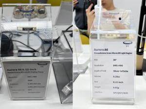
In the Micro LED ultra-clean laboratory of Guoxing Optoelectronics Research Institute, several precision equipment are operating in an orderly and efficient manner. The R & D staff wearing anti-static clothing were concentrating on monitoring the constantly beating real-time parameters on the display screen and carefully analyzing the subtle changes in the data. Micro LED, as a new display technology that films, miniaturizes, and arrays LED structures, its size is only in the range of 1 to 100 microns. These tiny LED chips can be directly integrated into the screen panel, thereby achieving high-precision and high-brightness display of images and bringing a qualitative leap to the visual experience.
![[Technical Self-improvement] Look at the](https://www.52dp.com/d/file/p/2025/03-03/52dp_1740986241456.jpg)
However, the smaller the size of the LED chip, the packaging difficulty it faces increases exponentially. In particular, the difficulty of accurately transferring millions of micron Micro LED chips to the target substrate and completing soldering is no different from building a tall building on fine sand. Among them, the huge amount of bonding has become an insurmountable gap that hinders the large-scale application of Micro LED technology.
As an innovative pioneer in LED packaging technology, Guoxing Optoelectronics has not backed down in the face of problems, but actively explores ways to break the situation. Faced with the dilemma that the single die reflow bonding method used in traditional flip chips cannot meet the huge bonding needs of Micro LED chips (less than 100 microns), Guoxing Optoelectronics has provided a solution with practical actions. By independently building a Micro LED technology platform, we carry out verification work on massive planar hot-pressing bonding processes, and strive to break through this technical bottleneck.
This new process first attaches the Micro LED chip array to the target substrate, and then performs eutectic bonding through heating and pressure. In order to ensure the accuracy of the bonding effect, Guoxing Optoelectronics uses a high-precision alignment system and a constant temperature heating system to accurately control the temperature and time, thereby achieving high-precision, high-density and high-efficiency electrical interconnection between the Micro LED chip and the target substrate.
After countless repeated polishing and verification, Guoxing Optoelectronics has achieved remarkable results based on the independently developed planar hot-pressing massive bonding process: in terms of high-density bonding, it can realize the bonding of tens of thousands of chips at a time., greatly improving the number and efficiency of bonding, and the one-time bond yield is as high as more than 99.99%; in terms of high-precision bonding, the bonding accuracy reaches± 2 microns, far better than the traditional± 20 microns; In terms of high-uniformity bonding, the temperature is evenly heated and the plane temperature difference is less than 5℃, which effectively ensures the stability of the bonding quality. In the whole research and development process, Guoxing Optoelectronics has undergone thousands of experiments, continuously optimized materials and process parameters, and finally successfully broke through the shackles of traditional packaging technology, overcome the key problems of Micro LED packaging mass bonding technology, and provided high yield, high precision and high efficiency for industrial innovation. Technical solutions.
![[Technical Self-improvement] See Micro LED](https://www.52dp.com/d/file/p/2025/03-03/52dp_1740986241251.jpg)
In recent years, Micro LED technology has gradually demonstrated unique advantages in many fields such as smart wearable devices, ultra-large size TVs, and augmented reality (AR). Not only that, it will also have broad application prospects in transparent displays, smart lights and more emerging scenarios in the future, with huge market potential. In order to firmly seize this market opportunity, Guoxing Optoelectronics closely focuses on the development strategic needs of the new display industry, relies on important innovation platforms such as the Mini Micro LED Research Center and the Guangdong Provincial Key Laboratory of Semiconductor Micro Display, and focuses on national key R & D plans and projects, Guangdong Province's R & D plans in key areas, and strives to build a set of innovation chains covering material epitaxy, chip manufacturing, transfer integration, full-color packaging and other aspects. By gathering the strength of industry, academia and research, targeting key core technologies, focusing on clearing blockages, eliminating pain points, and solving difficulties, we will comprehensively and deeply promote the R & D, innovation and industrial application of Micro LED technology.
Driven by the strong driving force of innovation, Guoxing Optoelectronics has achieved many key technological breakthroughs in the field of Micro LEDs. So far, more than 250 Mini/Micro LED patents have been applied for, among which they have won the China Patent Gold Medal for their full-color light-emitting device and display module patents. Through the layout of high-value patents, Guoxing Optoelectronics has achieved technological autonomy and controllability in core aspects such as chip packaging and massive transfer, and has successfully established a relatively complete ultra-high definition display packaging technology system.
However, in the face of the remarkable achievements it has made, Guoxing Optoelectronics has not slackened in the slightest and is still moving forward bravely on the road of innovation. The R & D staff of Guoxing Optoelectronics 'Micro LED project team have firm and passionate eyes, saying: In the next step, we will continue to explore the application potential of Micro LEDs in emerging fields such as indoor large-screen displays and intelligent car lights, and accelerate the research and development of key core technologies in this field. The research process will contribute greater strength to promoting the industrial application of Micro LED technology! quot;
![[Technical Self-improvement] Look at the](https://www.52dp.com/d/file/p/2025/03-03/52dp_1740986241603.jpg)
In 2025, Guoxing Optoelectronics will focus on value creation and launch a new round of activities to climb the peak. Under the guidance of the Group's FAITH business philosophy, Guoxing Optoelectronics 'innovative achievements will continue to emerge like bamboo shoots after rain, the development speed will continue to accelerate, and the grand blueprint of the modern industry will become clearer. I believe that in the near future, the goal of recreating a new national star will surely become a reality. National Star Optoelectronics will shine more brightly in the Micro LED field and even the entire display industry, writing its own glorious chapter.
Break through the technical blockade and bravely break through difficulties
In the Micro LED ultra-clean laboratory of Guoxing Optoelectronics Research Institute, several precision equipment are operating in an orderly and efficient manner. The R & D staff wearing anti-static clothing were concentrating on monitoring the constantly beating real-time parameters on the display screen and carefully analyzing the subtle changes in the data. Micro LED, as a new display technology that films, miniaturizes, and arrays LED structures, its size is only in the range of 1 to 100 microns. These tiny LED chips can be directly integrated into the screen panel, thereby achieving high-precision and high-brightness display of images and bringing a qualitative leap to the visual experience.
However, the smaller the size of the LED chip, the packaging difficulty it faces increases exponentially. In particular, the difficulty of accurately transferring millions of micron Micro LED chips to the target substrate and completing soldering is no different from building a tall building on fine sand. Among them, the huge amount of bonding has become an insurmountable gap that hinders the large-scale application of Micro LED technology.
As an innovative pioneer in LED packaging technology, Guoxing Optoelectronics has not backed down in the face of problems, but actively explores ways to break the situation. Faced with the dilemma that the single die reflow bonding method used in traditional flip chips cannot meet the huge bonding needs of Micro LED chips (less than 100 microns), Guoxing Optoelectronics has provided a solution with practical actions. By independently building a Micro LED technology platform, we carry out verification work on massive planar hot-pressing bonding processes, and strive to break through this technical bottleneck.
This new process first attaches the Micro LED chip array to the target substrate, and then performs eutectic bonding through heating and pressure. In order to ensure the accuracy of the bonding effect, Guoxing Optoelectronics uses a high-precision alignment system and a constant temperature heating system to accurately control the temperature and time, thereby achieving high-precision, high-density and high-efficiency electrical interconnection between the Micro LED chip and the target substrate.
After countless repeated polishing and verification, Guoxing Optoelectronics has achieved remarkable results based on the independently developed planar hot-pressing massive bonding process: in terms of high-density bonding, it can realize the bonding of tens of thousands of chips at a time., greatly improving the number and efficiency of bonding, and the one-time bond yield is as high as more than 99.99%; in terms of high-precision bonding, the bonding accuracy reaches± 2 microns, far better than the traditional± 20 microns; In terms of high-uniformity bonding, the temperature is evenly heated and the plane temperature difference is less than 5℃, which effectively ensures the stability of the bonding quality. In the whole research and development process, Guoxing Optoelectronics has undergone thousands of experiments, continuously optimized materials and process parameters, and finally successfully broke through the shackles of traditional packaging technology, overcome the key problems of Micro LED packaging mass bonding technology, and provided high yield, high precision and high efficiency for industrial innovation. Technical solutions.
Focus on innovation drive and move forward steadily
In recent years, Micro LED technology has gradually demonstrated unique advantages in many fields such as smart wearable devices, ultra-large size TVs, and augmented reality (AR). Not only that, it will also have broad application prospects in transparent displays, smart lights and more emerging scenarios in the future, with huge market potential. In order to firmly seize this market opportunity, Guoxing Optoelectronics closely focuses on the development strategic needs of the new display industry, relies on important innovation platforms such as the Mini Micro LED Research Center and the Guangdong Provincial Key Laboratory of Semiconductor Micro Display, and focuses on national key R & D plans and projects, Guangdong Province's R & D plans in key areas, and strives to build a set of innovation chains covering material epitaxy, chip manufacturing, transfer integration, full-color packaging and other aspects. By gathering the strength of industry, academia and research, targeting key core technologies, focusing on clearing blockages, eliminating pain points, and solving difficulties, we will comprehensively and deeply promote the R & D, innovation and industrial application of Micro LED technology.
Driven by the strong driving force of innovation, Guoxing Optoelectronics has achieved many key technological breakthroughs in the field of Micro LEDs. So far, more than 250 Mini/Micro LED patents have been applied for, among which they have won the China Patent Gold Medal for their full-color light-emitting device and display module patents. Through the layout of high-value patents, Guoxing Optoelectronics has achieved technological autonomy and controllability in core aspects such as chip packaging and massive transfer, and has successfully established a relatively complete ultra-high definition display packaging technology system.
However, in the face of the remarkable achievements it has made, Guoxing Optoelectronics has not slackened in the slightest and is still moving forward bravely on the road of innovation. The R & D staff of Guoxing Optoelectronics 'Micro LED project team have firm and passionate eyes, saying: In the next step, we will continue to explore the application potential of Micro LEDs in emerging fields such as indoor large-screen displays and intelligent car lights, and accelerate the research and development of key core technologies in this field. The research process will contribute greater strength to promoting the industrial application of Micro LED technology! quot;
Looking to the future and moving towards new heights
In 2025, Guoxing Optoelectronics will focus on value creation and launch a new round of activities to climb the peak. Under the guidance of the Group's FAITH business philosophy, Guoxing Optoelectronics 'innovative achievements will continue to emerge like bamboo shoots after rain, the development speed will continue to accelerate, and the grand blueprint of the modern industry will become clearer. I believe that in the near future, the goal of recreating a new national star will surely become a reality. National Star Optoelectronics will shine more brightly in the Micro LED field and even the entire display industry, writing its own glorious chapter.
TAG:
Guess you want to see it


Popular information
-
CEO of TV IKLAN Group, Indonesia's largest media company, led a delegation to inspect MNLED and the

-
Zhouming Technology shines in ISLE 2025, leading the innovation trend of LED light displays
-
Shijue Guangxu joins hands with industry partners to open a new chapter of cooperation with high-end

-
The LED spherical screen of the Lehman Combo Exhibition lights up the Junan Science and Technology M

-
2024 Global Music Tour: How does Redio dominate the C position of the global tour stage

-
Skyworth TV Spring Launch Conference: G7F Pro breaks the Mini LED technical problem
-
Lehman Optoelectronics: The road to intellectual property rights protection and the light of COB tec
-
Lehman Appears at the 25th China High-Speed Exhibition to Help Digital Upgrade of Smart Transportati
-
Zhouming Technology and Perfect World officially reached an educational ecological partnership!
-
Meta releases three smart glasses, and iteration of display technology pushes AI glasses to new heig

the charts
- CEO of TV IKLAN Group, Indonesia's largest media company, led a delegation to inspect MNLED and the
- Innolux joins hands with Yuantai, TPV and others to introduce large size color electronic paper into
- Xida Electronics signs a strategic cooperation agreement with Changbai Mountain Chixi District Manag
- Liard joins hands with "Three-Body" to open a new era of science fiction drama in China
- Zhaochi Semiconductor joins hands with Li Xing Semiconductor. Want to do big things?
- Zhou Ming joins hands with the Guangdong Basketball Association to produce another masterpiece! The
- ISE2023 Abbison's first exhibition in the new year has received frequent good news, and the immersiv
- Samsung Display and APS "work together" to create 3500ppi Micro OLED
- Zhouming Technology and Perfect World officially reached an educational ecological partnership!
- Longli Technology:Mini-LED has been shipped in batches to some in-vehicle customers, VR customers, e