Zhejiang University team made a major breakthrough in perovskite LED research
- author:
- 2025-03-21 14:48:47
Recently, the scientific research team led by Professor Di Dawei and Professor Zhao Baodan of Zhejiang University published an important paper entitled Downscaling micro- and nano-perovskite LEDs in the top academic journal "Nature""", which aroused thousands of waves in the field of LED research.
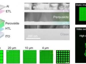
该团队成功研制出微米和纳米钙钛矿 LED(即 micro - 和 nano-PeLED),其像素尺寸跨度极大,从数百微米一直缩小至 90 纳米,堪称目前公开报道中尺寸最小的 LED 像素。Not only that, the team also built a pixel array with a pixel density of up to 127,000 PPI, setting a new resolution record for all types of LED arrays and reaching an ultra-high resolution level. The paper pointed out that Micro-LEDs based on III-V semiconductors are facing many challenges. On the one hand, manufacturing costs remain high. On the other hand, when the pixel size is reduced to about 10 microns or even less, its efficiency will decline sharply. In sharp contrast, perovskite LEDs (PeLEDs) show excellent performance with their lower processing costs. Since the demonstration of room temperature electroluminescence (EL) in halide perovskites in 2014, the performance of related devices has continued to make substantial breakthroughs. Today, their external quantum efficiency (EQEs) has reached 20 - 30%, and their working life has gradually approached organic LEDs.
In terms of technological innovation, the team pioneered a local contact process.
在技术创新方面,该团队开创性地提出了一种局域接触工艺。By introducing lithographically fabricated patterned windows in the additional insulating layer, it is ensured that the pixel area remains at a certain distance from the electrode edge. This innovative measure is of great significance and effectively avoids the problem of non-radiative energy loss caused by the exposure of perovskite materials to the edge of the electrode, thereby reducing LED efficiency. Based on this strategy, the team successfully manufactured green and near-infrared perovskite LEDs. Experimental data shows that the size reduction effect begins to show when the pixel size is reduced to a very small scale of about 180 nanometers, when the efficiency of the nano-PeLED drops to 50% of the maximum value. This result fully demonstrates that in the ultra-small size range, micro and nano-PeLEDs have significant advantages in efficiency compared to Micro-LEDs based on III-V semiconductors. The efficiency of the latter will be significantly reduced when the size is below 10 microns.
What is particularly eye-catching is that the team successfully developed the smallest size LED device currently, with a pixel density of up to 127,000 PPI, ranking first in terms of LED array resolution.
尤为引人注目的是,该团队成功研发出当前尺寸最小的 LED 器件,像素密度高达 127,000 PPI,在 LED 阵列分辨率方面独占鳌头。In addition, the team successfully developed a prototype active matrix micro-PeLED display relying on commercial thin film transistor (TFT) arrays, which effectively verified the huge application potential of micro -and nano-PeLEDs in the field of high-resolution displays. Through testing the stability of the device and research on the prototype active matrix micro PeLED display, a solid foundation has been laid for its future practical application. This research result of the Zhejiang University team is expected to open up a new path for the development of LED technology and promote related industries to a new stage of development.
TAG:
Guess you want to see it

Popular information
-
CEO of TV IKLAN Group, Indonesia's largest media company, led a delegation to inspect MNLED and the

-
Skyworth Commercial's innovative display at ISLE 2025 International Smart Display Exhibition
-
Video wall renewal in summer: Two new LCD video walls!

-
Kalette: The journey to compete in overseas markets, and the strength shines with glory
-
Grayscale technology shines in InfoComm Asia 2024, leading a new trend in display control technology
-
Alto Electronics helps Amazon Cloud Technology AWS build a new virtual reality studio XR Studio
-
Zhouming Technology and iQiyi: Bright double stars in the field of virtual production, leading the w
-
Sitan Technology shines at CES 2025, leading the new trend in Micro-LED technology
-
Guoxing Optoelectronics shines at the Shanghai International Automobile Lighting Exhibition to demon
-
Liard·Virtual Moving Point: High-precision Escort Robot Games

the charts
- CEO of TV IKLAN Group, Indonesia's largest media company, led a delegation to inspect MNLED and the
- Innolux joins hands with Yuantai, TPV and others to introduce large size color electronic paper into
- Xida Electronics signs a strategic cooperation agreement with Changbai Mountain Chixi District Manag
- Liard joins hands with "Three-Body" to open a new era of science fiction drama in China
- Zhaochi Semiconductor joins hands with Li Xing Semiconductor. Want to do big things?
- Zhou Ming joins hands with the Guangdong Basketball Association to produce another masterpiece! The
- ISE2023 Abbison's first exhibition in the new year has received frequent good news, and the immersiv
- Samsung Display and APS "work together" to create 3500ppi Micro OLED
- Zhouming Technology and Perfect World officially reached an educational ecological partnership!
- Longli Technology:Mini-LED has been shipped in batches to some in-vehicle customers, VR customers, e