Zhaochi Semiconductor's three Micro LED patents are moving towards authorization, lighting up a new
- author:
- 2025-05-20 09:34:49
In the wave of accelerated iteration of global display technology, Micro LEDs have become the focus of industry competition due to their advantages such as high brightness, low power consumption, and long life. As a core player in the Micro LED track, Zhaochi Semiconductor has recently ushered in a concentrated explosion of patent achievements thanks to its continuous technical cultivation-three key patents have entered the authorization stage simultaneously. This breakthrough not only injects strong impetus into the company's own development, but also provides new ideas for the technological upgrade of the entire Micro LED industry.
在 4 月 1 日踏入有效授权进程的 "Micro LED 外延片及其制备方法、Micro LED 芯片" 专利,聚焦于光电技术领域的关键环节。This patent innovatively constructs a special epitaxial wafer structure, in which buffer layers, N-type GaN layers, multiple quantum well layers and P-type GaN layers are stacked in an orderly manner on the substrate. Among them, the multi-quantum well layer is carefully designed into three parts: the first multi-quantum well layer is formed by alternately laminating the first InGaN quantum well layer, the first AlGaN/GaN superlattice layer and the first GaN quantum barrier layer; The second multi-quantum well layer is cyclically constructed using the second InGaN quantum well layer, the second AlGaN/GaN superlattice layer and the second GaN quantum barrier layer as the basic unit; the third multi-quantum well layer is formed by combining the third InGaN quantum well layer, the hole injection layer and the third GaN quantum barrier layer. This unique design effectively improves the light efficiency of Micro LED chips at low operating current densities, opening up a new path for energy-saving and efficient display applications.
早在 3 月 18 日,兆驰半导体的另外两项专利 --"Micro-LED 外延片及其制备方法、Micro-LED" 与 "高光效 Micro-LED 外延片及其制备方法、Micro-LED" 也已步入授权快车道,二者均致力于发光效率的突破。The former provides an N-type GaN layer, a first multi-quantum well layer and a P-type GaN layer on the substrate by precise control of the epitaxial wafer structure, wherein the quantum well layer and the first quantum barrier layer of the first multi-quantum well layer are alternately stacked, and the material composition and proportion of each sublayer are accurately designed, such as the increasing change in the In component proportion in the first InGaN layer and the decreasing trend of the Al component in the first AlGaN layer, both of which are tailored to optimize the luminescent performance. The latter creates a more complex and exquisite structure. Starting from the substrate, the buffer layer, the undoped GaN layer, the N-type GaN layer, the multi-quantum well layer, the hole extension layer, the hole storage layer and the hole layer are arranged in this order. It is worth mentioning that the three-layer functional structures all adopt periodic design. The hole expansion layer is alternately composed of BN layers and lightly Mg-doped GaN layers. The hole storage layer is composed of GaN layers, InGaN layers and Mg-doped AlGaN layers. The hole layer is periodically arranged by a P-type BInGaN layer, a Mg3N2 layer and a P-type GaN layer. This precise layout greatly improves the luminescent efficiency of the epitaxial wafer.
这三项专利的突破,是兆驰半导体长期技术积累与创新探索的缩影。With a deep understanding and continuous investment in Micro LED's core technology, the company not only establishes competitive barriers in technology research and development, but also provides a new technical model for the development of the industry through patent layout. With the gradual implementation of these patents, Zhaochi Semiconductor is expected to play a more important role in the future transformation of display technology, promoting Micro LED technology from the laboratory to a wider range of application scenarios, and bringing more disruptive innovations to the industry.
TAG:
Guess you want to see it


Popular information
-
CEO of TV IKLAN Group, Indonesia's largest media company, led a delegation to inspect MNLED and the

-
Abbison at the Osaka World Expo: The cultural narrative of LED display and industry breakthrough

-
Zhouming Technology: Light up the new dimension of Sanlitun movie viewing and reshape the new audio-
-
Alto Electronics: XR Studio, a brilliant chapter of media transformation and virtual production

-
Analysis of RGB-Mini LED TV Technology Competition Situation
-
AUO Optronics 'consolidated revenue in March 2025 was 25.9 billion yuan
-
Exploring Liard·Virtual Motion-point Mini AI holographic toy: The dream collision of technology and

-
Behind the Cambrian rise: Industrial confidence in domestic substitution

-
Lehman Optoelectronics shines with LED China, and the full-scene ecological layout demonstrates its

-
a picture reading| Zhaochi Shares 2024 Annual Report

the charts
- CEO of TV IKLAN Group, Indonesia's largest media company, led a delegation to inspect MNLED and the
- Innolux joins hands with Yuantai, TPV and others to introduce large size color electronic paper into
- Xida Electronics signs a strategic cooperation agreement with Changbai Mountain Chixi District Manag
- Liard joins hands with "Three-Body" to open a new era of science fiction drama in China
- Zhaochi Semiconductor joins hands with Li Xing Semiconductor. Want to do big things?
- Zhou Ming joins hands with the Guangdong Basketball Association to produce another masterpiece! The
- ISE2023 Abbison's first exhibition in the new year has received frequent good news, and the immersiv
- Samsung Display and APS "work together" to create 3500ppi Micro OLED
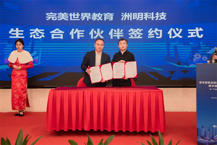
- Zhouming Technology and Perfect World officially reached an educational ecological partnership!
- Longli Technology:Mini-LED has been shipped in batches to some in-vehicle customers, VR customers, e