Guoxing Optoelectronics: LED reliability is protected by ultrasonic scanning
- author:
- 2025-10-31 17:41:08
As the core heart of display and lighting terminal products, whether LED devices have hidden defects such as voids and cracks inside directly determines the performance stability and service life of the terminal product. However, LED devices are small in size and precise in structure, and traditional detection methods are difficult to penetrate their packaging layers and accurately detect internal hidden dangers. As a leading enterprise in the field of LED packaging in China, Guoxing Optoelectronics has given a solution to break the situation. Relying on advanced ultrasonic scanning and testing technology, it uses non-destructive flaw detection to achieve accurate perspective of LED devices, building a solid reliability foundation for each device from the source, providing core guarantees for high-quality delivery of downstream terminal products.

Ultrasonic scanning testing: Industrial CT of LED devices, revealing the hidden details
In the field of LED device testing, ultrasonic scanning testing technology is like industrial CT. With its ability to non-destructive visualize the internal structure, it has become a key means to control the quality of the packaging process. It can penetrate the packaging material without disassembling the device, clearly presenting the internal microstructure, allowing micron-scale defects to be hidden.
Principle: High-frequency sound waves create perspective eyes, and echo signals draw internal maps
The core principle of ultrasonic scanning testing is to utilize the penetration and reflection characteristics of high-frequency ultrasonic waves: high-frequency sound waves (usually with frequencies up to tens of megahertz) are directionally emitted into the LED device. The sound waves will reflect at the interfaces of different materials (such as chips and bonding layers, encapsulation layers and substrates) and defects; these echo signals are received through high-precision sensors, and then converted into two-dimensional or three-dimensional images through algorithm processing, and finally a visual map of the internal structure of the device is generated. This method can not only clearly present the bonding state of the packaging layers, but also accurately locate the location, size and shape of small defects, providing an intuitive and scientific basis for process evaluation.
Goal: Focus on key aspects of packaging and target core quality risk points
Most of the reliability problems of LED devices stem from hidden defects in the packaging process. Guoxing Optoelectronics 'ultrasonic scanning testing focuses on three core testing targets: First, the chip bonding interface, to detect whether there are problems such as insufficient bonding and residual bubbles. Such defects can lead to reduced thermal conductivity and cause overheating and damage of the device; The second is the internal porosity of the material. Check whether there are tiny voids in the packaging compound and filling material, which will affect the light efficiency conduction and structural stability, and may cause crack expansion after long-term use; The third is the bonding state between the packaging layers to determine whether there is stratification phenomenon. The layering will destroy the sealing property of the device, lead to the intrusion of water vapor and impurities, and shorten the service life. Through accurate detection of these key links, core risks that affect device reliability are avoided from the source.
Ability: micron defect catcher, non-destructive testing ensures integrity
Compared with traditional inspection technology, the biggest advantages of ultrasonic scanning testing are its high accuracy and non-destructive nature. It can non-destructively detect internal voids, cracks and layered defects with a size of only microns (equivalent to a few tens of the diameter of a human hair), and the detection accuracy far exceeds the resolution limit between the naked eye and ordinary optical equipment. For example, in the inspection of a certain batch of LED devices, the ultrasonic scanning image clearly showed a void with a diameter of only 5 microns in the chip bonding layer (the colored area on the left). If such defects are not discovered in time, they will be affected by the device. Gradually expand during long-term work, eventually leading to chip shedding or functional failure. This ability to detect early and intervene early not only ensures the integrity of the device, but also avoids subsequent terminal product failures caused by defects.
Full life cycle applications: From R & D to mass production, dual defense lines protect quality
Guoxing Optoelectronics does not limit ultrasonic scanning testing to a single inspection link, but deeply integrates it into the entire life cycle of LED devices. It builds quality control defense lines in the R & D and mass production stages, and uses zero-defect standards to run through product design to delivery. The entire process.
R & D stage: Decision-making staff for process optimization and accelerating technology iteration
In the process of new product development and material introduction, ultrasonic scanning testing has become a key staff member of Guoxing Optoelectronics 'process optimization. The R & D team will conduct systematic ultrasonic scanning tests on device samples with different material combinations (such as different types of adhesives and packaging resins) and different process parameters (such as curing temperature and pressure), and analyze material compatibility by comparing internal structure images. and process rationality. For example, when testing a new type of high thermal conductivity adhesive, it was found that the internal porosity of the device was high at a specific curing temperature; by adjusting the temperature parameters and scanning and verification again, the process plan with the lowest porosity was finally found, which significantly improved the thermal conductivity of the device. Performance and reliability. This closed-loop model of test-analysis-optimization provides accurate data support for process iteration and accelerates the development process of high-reliability LED devices.
Mass production stage: Resident sentry for quality monitoring to prevent batch risks
After entering the mass production stage, ultrasonic scanning testing was incorporated into Guoxing Optoelectronics 'regular sampling and inspection process, becoming a monitoring platform for the stability of the production line process. The quality inspection team will regularly take samples from production batches for ultrasonic scanning in accordance with strict sampling standards to monitor the consistency of key processes such as chip bonding and packaging layer bonding in real time. Once a certain batch of samples is found to have an increasing defect rate, changes in process parameters will be immediately traced back, potential problems such as equipment and materials will be investigated, and the production process will be adjusted in a timely manner to avoid batch quality risks. For example, in the inspection of a certain batch of devices, it was found that the proportion of layered defects was slightly higher than the standard. Through traceability, it was found that it was caused by the deviation of the accuracy of the encapsulating glue coating equipment. After the equipment was calibrated in time, the defect rate quickly fell back to the acceptable range. This real-time monitoring and rapid response mechanism ensures that every batch of LED devices shipped can meet high reliability standards.
Comprehensive quality system: not only scanning, but also multi-dimensional escort industry upgrades
Ultrasonic scanning testing is only an important part of Guoxing Optoelectronics quality inspection system. In order to comprehensively ensure the quality of LED devices, the company has built a complete testing system covering multiple fields such as material analysis, optoelectronic performance, and thermal management. With full-dimensional and professional capabilities, it not only serves its own product innovation, but also empowers the entire LED industry chain. Quality improvement.
Platform-based testing capabilities: High-end equipment builds a hard core foundation
Guoxing Optoelectronics Analysis and Testing Center is equipped with a series of high-end testing equipment, forming multi-dimensional analysis capabilities: a scanning electron microscope can observe the microscopic topography of the surface and cross-section of the device, and accurately analyze the material composition and structure; an X-ray tester can penetrate through metal packaging to detect the connection status of internal chips and leads; an ultra-depth microscope can realize three-dimensional topography observation of small defects; In addition, there are optoelectronic performance testing systems, thermal resistance testing equipment, etc., which can comprehensively evaluate key indicators such as light efficiency, color coordinates, and thermal conductivity of LED devices. The collaborative application of these high-end equipment has built a complete inspection chain from microstructure to macro performance, providing hard-core technical support for product quality upgrades.
Professional service team: Senior experts assign precise value
The implementation of testing technology is inseparable from the support of professional talents. Guoxing Optoelectronics has established a testing team composed of senior management and technical experts in the industry. All members have many years of experience in LED packaging and testing, and are familiar with the causes and solutions of various defects. In actual testing, they can not only accurately identify defects, but also trace the root cause of the problem through data analysis. For example, in response to the problem of too fast light fading of the terminal product reported by a downstream customer, the team used ultrasonic scanning combined with thermal resistance testing to find that it was the internal cavity of the device. The cavity caused poor heat conduction, and then proposed suggestions to optimize the packaging process, helping the customer solve practical problems. This value-added service of testing + diagnosis + advice truly transforms testing data into value that improves product reliability.
Open service empowerment: nationally recognized laboratories help industry progress forward
Relying on the qualification of a nationally recognized laboratory (CNAS), Guoxing Optoelectronics Analysis and Testing Center also provides open testing services for the entire LED industry chain. Whether it is performance verification of upstream material suppliers, device selection testing of downstream terminal manufacturers, or technical research by scientific research institutions, you can use Guoxing Optoelectronics 'testing platform to obtain accurate data. For example, he once provided ultrasonic scanning testing services for the LED chip bonding process for a scientific research team in a university to help it complete relevant technical research; provided reliability testing of batch devices for many downstream lighting companies to help them screen high-quality suppliers. This open service model not only improves the overall testing efficiency of the industrial chain, but also uses accurate data to promote the improvement of industry quality standards and help the LED industry move towards high-end.
Conclusion: Based on reliability, leading the high-quality development of the LED industry
From a tiny LED device to display and lighting terminals throughout life scenes, reliability has always been the core lifeline of industrial development. With ultrasonic scanning and testing technology as its core, Guoxing Optoelectronics has built a quality assurance system covering the entire life cycle and multiple dimensions. It not only builds a solid foundation for reliability for its own products, but also provides stable and reliable core components for downstream terminal manufacturers. Empower industrial chain upgrades through open services.

As a domestic LED
TAG:
Guess you want to see it


Popular information
-
CEO of TV IKLAN Group, Indonesia's largest media company, led a delegation to inspect MNLED and the

-
AI glasses are in full swing, and giants are competing to enter the game to seize the new track

-
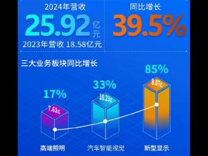
Jingke Electronics 'performance in 2024 is outstanding, with coordinated growth in multiple sectors
-
Abbison's road to breaking the situation in 2025: Taking products as the core, reconstructing the ne
-
Abbison: Lighting up sports venues with innovation and leading the new trend of LED display

-
Liard: An outstanding practitioner of the first-time economy, innovation drives change in multiple f

-
Guoxing Optoelectronics Xinli Electronics debuted at the 137th Canton Fair: Technology empowers ligh
-
Ruifeng Optoelectronics breaks through technological innovation and leads new changes in the electro
-
Zhou Ming Statement

-
Nova Nebula, Abison, BOE, and Lianjian Optoelectronics have their own highlights and challenges in i
the charts
- CEO of TV IKLAN Group, Indonesia's largest media company, led a delegation to inspect MNLED and the
- Innolux joins hands with Yuantai, TPV and others to introduce large size color electronic paper into
- Xida Electronics signs a strategic cooperation agreement with Changbai Mountain Chixi District Manag
- Liard joins hands with "Three-Body" to open a new era of science fiction drama in China
- Zhaochi Semiconductor joins hands with Li Xing Semiconductor. Want to do big things?
- Zhou Ming joins hands with the Guangdong Basketball Association to produce another masterpiece! The
- ISE2023 Abbison's first exhibition in the new year has received frequent good news, and the immersiv
- Samsung Display and APS "work together" to create 3500ppi Micro OLED
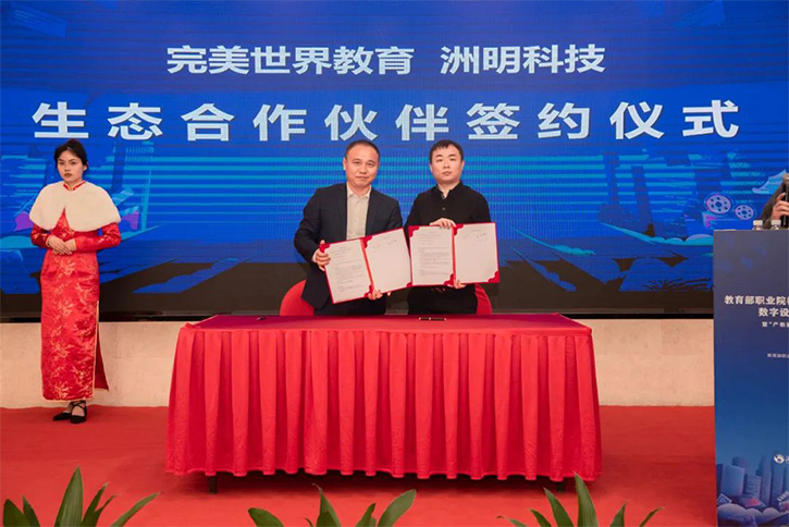
- Zhouming Technology and Perfect World officially reached an educational ecological partnership!
- Longli Technology:Mini-LED has been shipped in batches to some in-vehicle customers, VR customers, e