Micro LED technology innovation boom is surging: many companies have made patent breakthroughs focus
- author:
- 2025-05-30 16:21:23
Recently, there has been a wave of technological innovation in the field of Micro LED display. Companies such as Lehman Optoelectronics, Digital Optical Core, Yixin Semiconductor, and Inspur Huaguang have intensively publicized the progress of relevant patents, focusing on core links such as chip processing, epitaxial wafer structure, and massive transfer technology. The aim is to break through key performance bottlenecks such as light efficiency, light color, power and stability, and inject new momentum into the commercialization process of Micro LEDs.
In terms of electrode design, the chip adopts a" three-cathode + common cathode" structure, which can realize flexible switching of single chip red, green and blue luminescence, two-color mixed light and full-color luminescence. The light color adjustable range covers the Rec.2020 color gamut standard. 92% of the standard. This highly integrated design not only saves more than 30% of wafer area, reduces chip costs, but also simplifies the downstream module assembly process, providing technical support for large-scale mass production of ultra-high-definition display terminals.
During the preparation process, the direct interconnection between the source electrode of the MOS structure and the P electrode of the micro-LED unit is achieved by depositing a thick layer of ITO, eliminating the traditional bonding process and reducing the process steps by 40%. Experimental data shows that the driver chip using this technology has a response speed of nanoseconds and can support refresh rates above 200Hz. It is suitable for high-speed scenarios such as AR/VR near-eye displays, providing new ideas for the monolithic integration of Micro LEDs and driver circuits.

In the transfer process, the bottom packaging layer of the chip is selectively heated by laser, so that a single chip is separated from the first substrate and then accurately bonded to the second substrate. The positioning accuracy reaches± 1μ m, and the yield per transfer is increased to 99.98%. This method is suitable for the manufacturing of high-density pixel arrays with a pitch of less than 50 m, laying a foundation for the application of Micro LEDs in small size and high-resolution scenes such as smart watches and car displays.

By adjusting the inner diameter of the ring and the number of DBR periods, the angle can be further controlled in the range of 30° - 80°, effectively reducing the interference between adjacent pixels (crosstalk rate < 3%). Experiments show that the color purity of RGB chips using this structure is improved by 15%, and is suitable for scenarios with strict optical accuracy requirements such as near field display and naked-eye 3D, providing a technical path for the differentiated application of Micro LEDs in the high-end display field.
Lehman Optoelectronics: Full-color quantum dot chip technology achieves double breakthroughs in integration and efficiency On
May 27, Shenzhen Lehman Optoelectronics Technology Co., Ltd. teamed up with Huizhou Lehman Optoelectronics Technology Co., Ltd. to flip chip Micro LED full-color quantum dot chips, preparation methods and use patents were officially authorized. The invention innovatively builds a red, blue and green light-emitting structure on a single LED chip, breaking through the traditional RGB array layout model and significantly improving the transfer efficiency and yield of huge amounts. By integrating the quantum material layer, the chip's luminous stability is not affected by current fluctuations, and the color accuracy reaches a professional display level of △E<1.5.In terms of electrode design, the chip adopts a" three-cathode + common cathode" structure, which can realize flexible switching of single chip red, green and blue luminescence, two-color mixed light and full-color luminescence. The light color adjustable range covers the Rec.2020 color gamut standard. 92% of the standard. This highly integrated design not only saves more than 30% of wafer area, reduces chip costs, but also simplifies the downstream module assembly process, providing technical support for large-scale mass production of ultra-high-definition display terminals.
Digital optical core: Indium tin oxide MOS structure driving technology simplifies the preparation process On
May 16, Hunan University and Beijing Digital Optical Core Integrated Circuit Design Co., Ltd. jointly applied for a MOS structure driving micro-LED based on channel/contact dual-use indium tin oxide and the patent on the preparation method entered the stage of publication in the trial. This technology forms a thin layer of non-degenerate indium tin oxide (ITO) semiconductor channel and a thick layer of degenerate ITO contact electrode on the same substrate through a photolithography process, achieving low contact resistance (<10·cm ²) compatibility with high current density (> 10 ³A/cm ²) of the MOS driving unit.During the preparation process, the direct interconnection between the source electrode of the MOS structure and the P electrode of the micro-LED unit is achieved by depositing a thick layer of ITO, eliminating the traditional bonding process and reducing the process steps by 40%. Experimental data shows that the driver chip using this technology has a response speed of nanoseconds and can support refresh rates above 200Hz. It is suitable for high-speed scenarios such as AR/VR near-eye displays, providing new ideas for the monolithic integration of Micro LEDs and driver circuits.
Yixin Semiconductor: Hexagonal chip design improves massive transfer accuracy
On May 13, Suzhou Yixin Semiconductor Co., Ltd. Micro LED chip batch transfer method and application patents entered the stage of publication under review. Aiming at the pain points of traditional square chips with high sidewall proportion and difficulty in laser transfer, this technology adopts a hexagonal Micro LED chip design to reduce the sidewall area proportion from 35% to 22%, significantly reducing the stress concentration during laser lift-off. problem.In the transfer process, the bottom packaging layer of the chip is selectively heated by laser, so that a single chip is separated from the first substrate and then accurately bonded to the second substrate. The positioning accuracy reaches± 1μ m, and the yield per transfer is increased to 99.98%. This method is suitable for the manufacturing of high-density pixel arrays with a pitch of less than 50 m, laying a foundation for the application of Micro LEDs in small size and high-resolution scenes such as smart watches and car displays.
Inspur Huaguang: Ring electrode structure accurately controls light emitting angle
On May 9, Shandong Inspur Huaguang Optoelectronics Co., Ltd. was authorized for the preparation method of Micro LED chips to control light emitting angle. This technology designs a circular electrode structure so that current is injected from around the ring and conducted to the MQW (multiple quantum well) light-emitting layer in the ring through the ITO layer. The optical confinement effect of the ring electrode and the bottom DBR (distributed Bragg mirror) is utilized to compress the light output angle from the traditional 120 to less than 60.By adjusting the inner diameter of the ring and the number of DBR periods, the angle can be further controlled in the range of 30° - 80°, effectively reducing the interference between adjacent pixels (crosstalk rate < 3%). Experiments show that the color purity of RGB chips using this structure is improved by 15%, and is suitable for scenarios with strict optical accuracy requirements such as near field display and naked-eye 3D, providing a technical path for the differentiated application of Micro LEDs in the high-end display field.
Industry Impact and Trend Outlook The
above patent progress shows three major trends in Micro LED technology research and development:integration (single chip full color, driver integration),precision(transfer accuracy, optical control), andlow cost (process simplification, material innovation).). With the gradual breakthrough of core technology bottlenecks, Micro LED's penetration rate in high-end TVs, car displays, AR/VR and other fields is expected to accelerate. Industry insiders pointed out that differences in patent layout among enterprises are gradually forming technical barriers. In the future, patent competition around massive transfer, full-color, and driving solutions will become the focus of the market, and cross-enterprise technical collaboration and standard co-construction will become the key to industrial scale development.TAG:
Guess you want to see it


Popular information
-
CEO of TV IKLAN Group, Indonesia's largest media company, led a delegation to inspect MNLED and the

-
Decoding of Zhaochi's 2025 Q1 financial report: The road to industrial breakthrough driven by multi-
-
Guoxing Optoelectronics is deeply engaged in brand building and demonstrates the responsibility of s
-
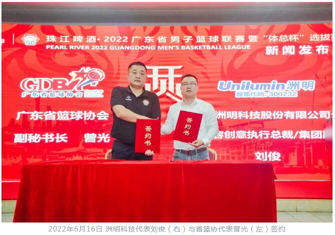
Zhou Ming joins hands with the Guangdong Basketball Association to produce another masterpiece! The
-
Empowering Liard! The country's largest humanoid robot training ground officially opened

-
The LED spherical screen of the Lehman Combo Exhibition lights up the Junan Science and Technology M

-
Zhaochi Group seeks change and breaks the situation: using all-dimensional innovation to draw a new
-
Zhaochi Group's 20-year glory: the transformation path from a cutting-edge industry to a technologic
-
TCL Huaxing Suzhou Base received AWS International Water Management Gold Certification, becoming the
-
Revenue increased by 4.2% year-on-year, and core product differentiation highlights are sufficient!

the charts
- CEO of TV IKLAN Group, Indonesia's largest media company, led a delegation to inspect MNLED and the
- Innolux joins hands with Yuantai, TPV and others to introduce large size color electronic paper into
- Xida Electronics signs a strategic cooperation agreement with Changbai Mountain Chixi District Manag
- Liard joins hands with "Three-Body" to open a new era of science fiction drama in China
- Zhaochi Semiconductor joins hands with Li Xing Semiconductor. Want to do big things?
- Zhou Ming joins hands with the Guangdong Basketball Association to produce another masterpiece! The
- ISE2023 Abbison's first exhibition in the new year has received frequent good news, and the immersiv
- Samsung Display and APS "work together" to create 3500ppi Micro OLED
- Zhouming Technology and Perfect World officially reached an educational ecological partnership!
- Longli Technology:Mini-LED has been shipped in batches to some in-vehicle customers, VR customers, e