Micro LED technology patents surge: Zhaochi, Gaoke Huaye, and Shuoxuan Semiconductor work together
- author:
- 2024-12-20 19:28:35
At a time when the wave of technology is surging and innovation competition is fierce, the Micro LED technology field is like a mysterious sea full of infinite possibilities, attracting many companies to set sail and explore the treasures therein. Entering December, a wave of eye-catching patents surged in this sea area. Companies such as Chizhao Semiconductor, Gaoke Huaye, Shuoxuan Semiconductor, and other companies are like brave navigators, successively announcing their patent achievements in Micro LEDs., covering core technologies such as MiP, massive transfer, and epitaxial wafers, has injected new vitality and hope into the entire industry, and also indicates that Micro LED technology is about to enter a new stage of development.
1. Gaoke Huaye: The innovative path to quantum dot MicroMIP device preparation
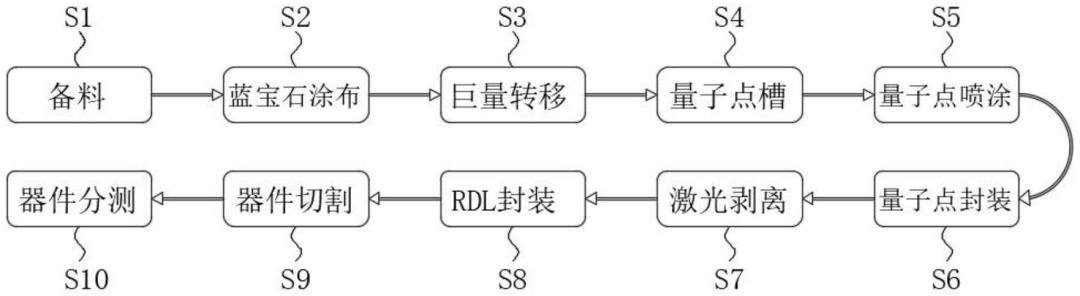
On December 10, Shanxi Gaoke Huaye Electronic Group Co., Ltd., like a skilled magician, announced" a patent related to a quantum dot MicroMIP device preparation method", and the patent has entered the stage of publication under review. This patent is like a mysterious magic book, detailing the wonderful steps for preparing quantum dot Micro MIP devices: starting with careful preparation of raw materials, as rigorous and meticulous as a magician collects magic materials; then applying sapphire coating to lay the foundation for subsequent magic display; then using massive transfer technology to efficiently and accurately transfer chips; and then creating quantum dot grooves to provide exclusive space for the magic of color conversion; Then quantum dot spraying is carried out to inject the magic of brilliant colors; then quantum dot packaging is implemented to protect the stability of this color magic; laser stripping technology is used to accurately remove excess parts, just like magic pruning; then RDL packaging is carried out to build internal connections. Magic channels; Finally, through device cutting and sub-testing, perfect quantum dot MicroMIP devices are born like magic treasures.
The subtlety of this patent is that it cleverly combines blue light Micro COW with quantum dot materials, as if a wonderful combination of two magic elements, achieving the magical effect of color conversion, thereby creating bright red light and green light., like adding more gorgeous color strokes to the picture scroll displaying quality, greatly improving the color saturation and delicacy of the display device, allowing the audience to see a more realistic and vivid picture through a magic window. At the same time, the use of massive transfer technology and laser lift-off technology makes the transfer and packaging process of chips more efficient and precise like precision operations in a magic workshop, effectively reducing losses in the manufacturing process, just like reducing magic energy. The unprovoked loss helps control manufacturing costs, and the cutting and packaging process of the device has also been carefully optimized, just like creating an exquisite shell for a magic treasure, ensuring the performance and quality of the device. At the same time, production efficiency is greatly improved, paving a solid path for large-scale production and widespread application of quantum dot MicroMIP devices.
2. Jiangxi Zhaochi Semiconductor: Overcoming Micro LED technical problems in multiple dimensions
According to news from the enterprise investigation, Jiangxi Zhaochi Semiconductor Co., Ltd. was like a generalist inventor in December and announced four Micro LED-related patents, covering Micro LED technology in all aspects, from epitaxial wafer structure to preparation method. In-depth exploration and innovation.
(1) Cheats on improving light efficiency yield of blue light Micro-LED epitaxial wafers
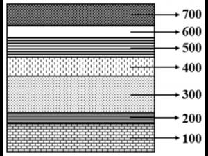
On December 10," the patent for an epitaxial wafer and its preparation method for a blue Micro-LED" successfully entered the authorization stage. This patent goes deep into the mysterious forest in the field of semiconductor materials technology and unearth the unique structural secrets of blue Micro-LED epitaxial wafers. The multi-quantum well light-emitting layer in its epitaxial wafer is like a carefully constructed multi-layer magic tower, including a first light blue multi-quantum well layer, a second light blue multi-quantum well layer, and a third light blue multi-quantum well layer that are sequentially grown in layers. The quantum well layer and the fourth light blue multi-quantum well layer. Among them, the first shallow blue light multi-quantum well layer is a superlattice structure of the first InGaN multi-quantum well layer and the first multi-quantum well compound barrier layer that grow alternately in turn, as if it is the first cornerstone of the Magic Tower, laying a unique optical foundation; the second light blue light multi-quantum well layer is a superlattice of similar structure, further strengthening the foundation; The third blue multi-quantum well layer is a superlattice structure of the third InGaN multi-quantum well layer and the Si-doped GaN-doped multi-quantum barrier layer that grow alternately in turn, just like the core energy layer of the Magic Tower, providing key blue light emission; The fourth blue light multi-quantum well layer is a corresponding superlattice structure to improve the overall performance.
Implementing this invention is like activating the energy amplifier of the Magic Tower, which can significantly improve the light efficiency and yield of the Micro-LED under low working current density, so that the Micro-LED device can still maintain excellent performance when operating with low power consumption. The luminous performance opens a broad door for its application in various energy-saving display devices, such as smartphones, wearable devices, etc., allowing these devices to effectively extend battery life while displaying gorgeous pictures. Improve user experience.
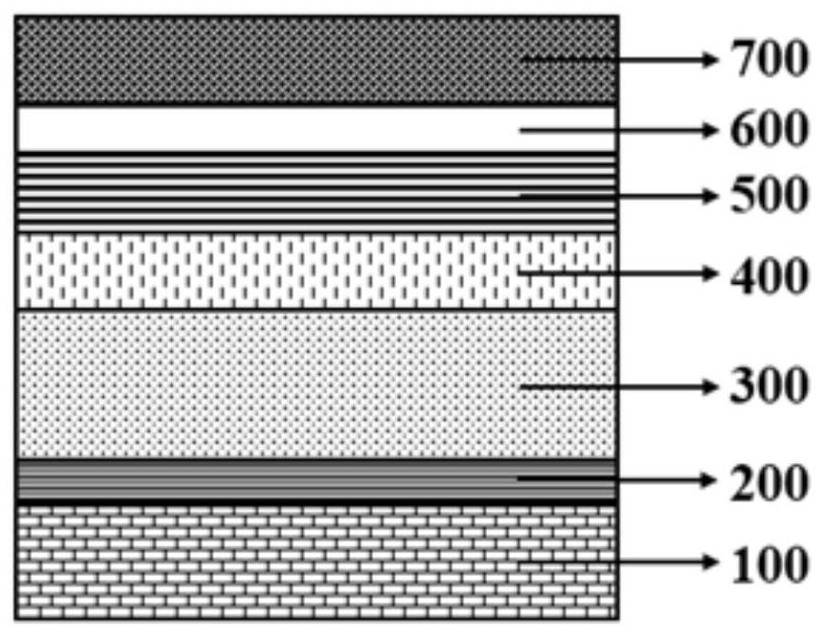
(2) Optimization of the performance of blue Micro-LED epitaxial structure
Also on December 10," a patent on the epitaxial structure and preparation method of a blue Micro-LED" also entered the authorization stage. The patent focuses on another key perspective in the field of semiconductor materials technology, revealing the epitaxial structure of a blue Micro-LED and the exquisite process for its preparation. Its epitaxial structure includes a substrate, a buffer layer, an N-type semiconductor layer, a low-temperature stress relief layer, a multi-quantum well light-emitting layer, an electron blocking layer and a P-type semiconductor layer stacked in order on the substrate. This series of structures is like a collaborative magic team. Among them, the multi-quantum well light-emitting layer includes a first shallow blue light multi-quantum well sublayer, a second light blue light multi-quantum well sublayer, a third blue light multi-quantum well sublayer and a fourth light blue light multi-quantum well sublayer that are stacked and grown in order from bottom to top. Light multi-quantum well sublayer, and each sublayer is a superlattice structure of InGaN multi-quantum well layers and multi-quantum barrier layers, just like each member of the team with unique skills, cooperating with each other.
Implementing the invention seems to equip the magic team with a top coordinating commander, which can effectively reduce the stress when growing InGaN quantum wells, just like eliminating friction and conflicts within the team, significantly improving the quality of the multi-quantum well light-emitting layer, and at the same time improving the P-type The hole injection efficiency of the semiconductor layer is like injecting a strong source of power into the team, thereby improving the performance of the Micro-LED chip under low working current density, and is especially suitable for small size, Low-current and low-power blue-light Micro-LED application scenarios, such as micro displays, high-definition camera viewfinders, etc., provide high-performance Micro-LED solutions for these tiny but extremely demanding devices.
(3) Crystal quality and efficiency improvement strategies for Micro-LED epitaxial structures
On December 3," a patent on the epitaxial structure and preparation method of a Micro-LED" entered the authorization stage. This patent goes deep into the technical field of semiconductor materials and explores a new Micro-LED epitaxial structure and its preparation path. The epitaxial structure comprises a substrate, a buffer layer, an undoped GaN layer, an N-type doped GaN layer, an insertion layer, a multiple quantum well layer, an electron blocking layer, a P-type doped GaN layer and a contact layer, which are sequentially stacked on the substrate, wherein the insertion layer is like a mysterious magic intermediary, including an AlN layer, a patterned GaSb layer, an Al metal layer and an InGaN layer arranged in sequence on the N-type doped GaN layer.
Providing an insertion layer between the N-type doped GaN layer and the multi-quantum well layer seems to add a stabilizer to the magic energy transmission line, which can reduce the stress when growing the multi-quantum well layer and reduce the dislocation density of the multi-quantum well layer., like eliminating interference and loss in energy transmission, improving the crystal quality of the multi-quantum well layer, thereby improving the internal quantum efficiency of the Micro LED, reducing the working voltage, and improving the luminous brightness. This enables Micro-LEDs to emit brighter and clearer light at lower energy consumption. Whether it is in application scenarios such as large outdoor displays or indoor high-definition TVs, it can show excellent visual effects and reduce energy consumption., in line with the dual needs of modern society for energy conservation, environmental protection and high-quality display.
(4) Efficiency improvement password for low-voltage Micro-LED epitaxial wafers
On December 3," the low-voltage Micro-LED epitaxial wafer and its preparation method, and Micro-LED" patents entered the stage of publication during trial. This patent discloses a low-voltage Micro LED epitaxial wafer and its preparation method. Micro-LED is a mysterious treasure house in the field of semiconductor optoelectronic devices. The low-voltage Micro LED epitaxial wafer sequentially comprises a substrate, a buffer layer, an undoped GaN layer, an N-type GaN layer, a multiple quantum well layer, an electron barrier layer, a P-type GaN layer and a P-type contact layer, wherein the P-type contact layer is like a carefully improved magic interface, including a porous AlInN layer, a two-dimensional P-type BGaN layer, an AlN roughening layer, a P-type BInGaN nanocluster layer and a P-type AlInGaN roughening layer stacked on the P-type GaN layer in sequence. and the porous AlInN layer is made by etching the AlInN layer with H2, and the P-type AlInGaN roughening layer is made by roughening the P-type AlInGaN layer with N2.
Implementing the invention is like installing an efficient voltage regulation magic device for Micro-LED equipment, which can reduce the working voltage and improve light extraction efficiency, thereby improving luminous efficiency. This makes Micro-LEDs more advantageous in the application of various portable electronic devices, such as tablets, notebooks, etc., which can provide a more lasting, brighter and clearer display effect under limited battery capacity to meet users. High requirements for display quality in mobile office, entertainment and other scenarios.
3. Anhui Shuoxuan Semiconductor: Breakthroughs in energy conservation and uniformity of Micro-LED display drivers
On December 10, Anhui Shuoxuan Semiconductor Co., Ltd. announced" that a patent related to a driving method and chip for Micro-LED displays" has entered the stage of publication under trial. This patent is like a smart navigator, for Micro-LED
TAG:
Guess you want to see it


Popular information
-
Sharp launches a 42-inch e-ink screen poster: it can be displayed even when power is turned off
-
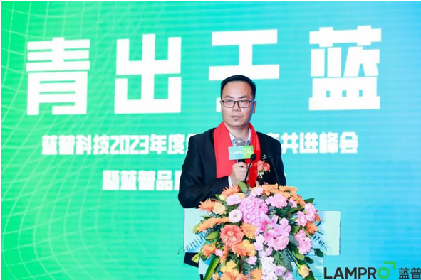
Zhouming Group's Lampu brand renewal and upgrade have been released!
-
TCL Huaxing showcases the world's first 65-inch 8K printed OLED display
-
South Korea launches Ex-OLED strategy to ensure leapfrog technology
-
Sony launches new Crystal LED black crystal BH and CH series small-pitch LED displays launched in Ap

-
The world's first 120-inch 4K Mini LED direct-display super TV
-
South Korean university research team proposes thin film transistor technology to improve the perfor

-
The OLED TV market has exploded 1500 times in 10 years: it will exceed 10 million units in three yea
-
Micro LED technology patents surge: Zhaochi, Gaoke Huaye, and Shuoxuan Semiconductor work together
-
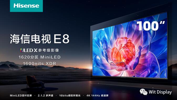
Hisense released a 100-inch thousand-level zone TV E8K, opening a new era of 100-inch giant screens
the charts
- The OLED TV market has exploded 1500 times in 10 years: it will exceed 10 million units in three yea
- The world's first 120-inch 4K Mini LED direct-display super TV
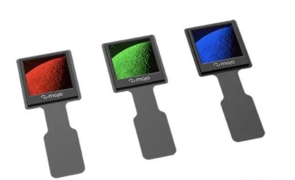
- Mojo Vision develops the world's highest density Micro LEDs
- Zhouming Group's Lampu brand renewal and upgrade have been released!
- First in Europe! Sony Black Crystal virtual production studio completed
- Zhaochi Semiconductor: Announced two invention patents related to Micro LED chips
- South Korean university research team proposes thin film transistor technology to improve the perfor
- South Korea launches Ex-OLED strategy to ensure leapfrog technology
- Sony launches new Crystal LED black crystal BH and CH series small-pitch LED displays launched in Ap
- Changhong released 8K high brush Mini-LED TV