Four Micro LED technologies achieve new progress
- author:
- 2024-06-04 14:59:52
Recently, Micro LED technology has become increasingly dynamic, as follows:
Samsunghas obtained patents on"micro LED displays and their manufacturing methods".
The team of the Korea Academy of Science and Technology has developed amicrovacuum assisted selective transfer (VAST) technology that transfers a large number of microled chips by adjusting the microvacuum suction.
A research team at Shanghai University has developednew chip bonding technology to improve the performance of Micro LEDs.
Chongqing Zhongke Yaolu Boat Information Technology Co., Ltd. has developedMicro LED wafer inspection equipment, which can solve bottleneck problems such as difficulty in accurately transferring huge amounts of chips and difficulty in detecting defective dots, and accelerate the mass production process of Micro LED displays.
01. Samsung: Obtained patent for Micro LED micro display
On December 20, according to an announcement by the State Intellectual Property Office, Samsung Electronics Co., Ltd. obtained an invention patent entitled"Micro LED Display and its Manufacturing Method", authorization announcement number CN110870066B, and the application date is June 2018.

Source State Intellectual Property Office
The patent abstract shows that this disclosure describes a miniature light emitting diode (LED) display. The display may include a printed circuit board (PCB) including a plurality of solder pads, a micro LED package includinga plurality of micro LED chips, and a plurality of solder electrodes bonding the micro LED chips to the solder pads of the PCB. After attaching the micro LED chips to the carrier film, the micro LED packages can be rearranged on the temporary fixing film in a red-green-blue (RGB) state using a pickup device according to the display pixel configuration.
02. KAIST research team demonstrated Micro LED selective transfer printing technology
On December 19, foreign media reported that the KAIST research team led by Professor Keon Jae Lee demonstrated the selective modulation of micro-vacuum forces to transfer and print a large number of micro inorganic semiconductor chips.

The concept of micro-vacuum assisted selective transfer (VAST), source of KAIST
It is reported that this key technology relies on the laser-induced etching (LIE) method to form a20-m-sized micro hole array with a high aspect ratio on a glass substrate at a manufacturing speed of up to 7000 holes per second. LIE drilled glass is connected to vacuum channels that control the microvacuum force at the required hole array to selectively pick up and release microLEDs.
Compared with previous transfer methods, micro-vacuum assisted transfer achieves higher adhesion switching performance, enables micro semiconductors with various foreign materials, size, shapes and thicknesses to be assembled on any substrate, and has a high transfer yield.

Universal transfer of thin film semiconductors through VAST, source by KAIST
It is worth mentioning that Professor Keon Jae Lee said that microvacuum-assisted transfer provides an interesting tool for large-scale and selective integration of micro-scale high-performance inorganic semiconductors. Currently, the team is studyingthe transfer printing of commercial microLED chips with ejector systems for the commercialization of next-generation displays (large-screen TVs, flexible/stretchable devices) and wearable phototherapy patches.
03. Shanghai University research team demonstrates new flip chip bonding technology
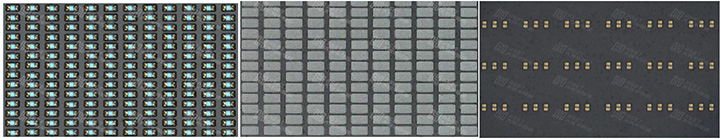
On December 18, a research team at Shanghai University recently demonstrated a technology that can improvethe integration and performance of micro MicroLED devicesused in next-generation displays.
It is understood that shrinking LEDs to miniature poses manufacturing and reliability obstacles, with core challenges including integrating MicroLED pixel arrays with silicon control circuits that operate displays. This integration technology is achieved through a flip-chip bonding process that physically and electronically connects the MicroLED chip to a bond plate on a silicon backplane. However, when the pixel size is reduced to less than 50 microns, this bonding interface can easily fail due to minute defects and mechanical stress.

Blue Micro LED manufacturing process using flip chips;(Source: AIP)
In response to this problem, the Shanghai University research team enhanced the flip-chip bonding process by using alayered gold-indium-gold (Au/In/Au) metal interlayerinstead of traditional pure indium bumps. The team used flip-chip bonding technology to connect the Micro LEDs to silicon at a mild temperature of 200C to avoid damage caused by mismatch between heating and cooling, while forming a highly conductive bond.
Compared with pure indium, the flip-chip bonding process with a multilayer metal interlayer of gold-indium-gold (Au/In/Au)reduceselectricalresistance by 40%, while also eliminating cracks and gaps on the bonding surface. Testing shear strength shows that the mechanical strength of the Au/In/Au bond is more than three times that of the original.
The research team integrated these layered connections into a 15 - 30-pixel Micro LED demonstration array with light sources sized 20 - 35 microns. As a result, these panels showed excellent display performance, including low operating voltages and record high brightness, reaching 1.78 million candelas per square meter.

FIB cross-section SEM images of indium bumps (a) and Au/In/Au multilayer films (b), and SEM images of blue Micro LED chips after flip chip bonding (c)
04.Rocket Ship Technology develops Micro LED wafer inspection equipment
On December 19, Chongqing Zhongke Yaoluan Information Technology Co., Ltd. said that it had successfully developed Micro LED wafer inspection equipment.
It is understood that the equipment will be applied tested on the production line of a domestic display panel companyin December 2023; if the test goes smoothly, it is expected to be put into use in the company in the first half of 2024.
The relevant person in charge of Yaoguan Technology said that after testing, in the chip inspection process, the missed detection rate of Micro LED chips by this Micro LED wafer inspection equipmentis less than 0.01%; in the chip transfer process, it can guide the chip transfer device to The chip transfer accuracy is controlled to a level ofless than 1 micron.
Based on this, this set of testing equipment can help display panel companies greatly improve the pixel yield of Micro LED displays, and control the number of chips that need to be repaired to a very low level, thereby significantly reducing the production cost of Micro LED displays and realizing Micro Large-scale commercialization of LED display technology.
TAG:
Guess you want to see it
Popular information
-
A team from Xiamen University designs artificial nanostructures that enhance deep ultraviolet light
-
Huge transfer and breakthrough: 75,000 MicroLEDs can be transferred at a time

-
Domestic R &D team develops Micro LED high-efficiency backlight devices
-
Analysis of huge transfer technology: How to break through the Micro LED display process problems?
-
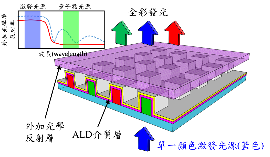
Apply materials to develop new Micro LED full-color technology
-
The best solution for AR glasses? Integrating Micro LEDs with advanced CMOS
-
Analysis of the evolution path of Samsung Display XR Display's MicroLED microdisplay technology
-
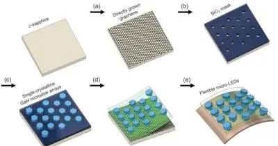
South Korean universities achieve growth of flexible GaN Micro LED arrays on graphene substrates
-
It can improve the light extraction rate of far-ultraviolet LEDs, and Silanna UV technology has beco
-
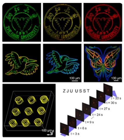
Zhejiang University's micro-level Micro-LED array achievements were selected into the top ten scient
the charts
- The best solution for AR glasses? Integrating Micro LEDs with advanced CMOS
- Red MicroLED R &D competition accelerates: Material innovation can solve the problem of luminous eff
- Micro LED heating capacity reduced by 40%! This study is supported by Samsung
- Zhejiang University's micro-level Micro-LED array achievements were selected into the top ten scient
- Red MicroLED R &D competition accelerates: Material innovation can solve the problem of luminous eff
- Analysis of huge transfer technology: How to break through the Micro LED display process problems?
- technology| Interpretation of MicroLED Technology in Mico Display Principles
- Micro LED achieves breakthrough results again
- Micro 0.4 released globally, opening a new era in the LED industry
- A team from Xiamen University designs artificial nanostructures that enhance deep ultraviolet light