It can improve the light extraction rate of far-ultraviolet LEDs, and Silanna UV technology has beco
- author:
- 2024-06-04 15:58:30
Recently, a research team at Silanna UV in Australia announced research using the properties of gallium nitride: aluminum nitride (GaN: AlN) short-period superlattice (SPSL), claiming that the radiation flux of Far-C UV LEDs grown on sapphire reached a record of 17.4mW.
AlGaN LEDs are the way to achieve low-cost, compact ultraviolet light sources
Although AlGaN LEDs are seen as a way to achieve low-cost, compact ultraviolet light sources, there are still many challenges to overcome. As the aluminum content in AlGaN increases, the light produced becomes more difficult to extract because the recombination process emits photons into the transverse magnetic (TM) mode rather than the transverse electric (TE) mode. Therefore, light is mainly emitted parallel rather than perpendicular to the device layers, and another problem with high aluminum content AlGaN is low doping efficiency.
In GaN, light emission tends to be perpendicular to the device layer, and the heavy hole (HH) band is the highest energy level, where electrons in the conduction band are mainly recombined. In contrast, in AlGaN with high aluminum content, the crystal field splitting hole (CH) band has the highest energy level, and electrons recombined into this band emit TM mode.

Figure 1: Valence band energy-quantity (E-k) plots along the c-axis for (a) bulk Al0.8Ga0.2N and (b) 1:4 single-layer GaN:AlN short-period superlattices (SPSL)(period L) calculated using 6x6k.p theory.
Different LED target wavelengths can be obtained by changing the SPSL layer thickness
To this end, Silanna UV team used the SPSL structure to restore the HH small band (HH1) to the highest energy level, thereby achieving TE light extraction. In addition, SPSL can also alleviate the problem of doping efficiency. The research team not only used SPSL to replace a part of the device structure, but used SPSL in almost the entire epitaxial material layer.
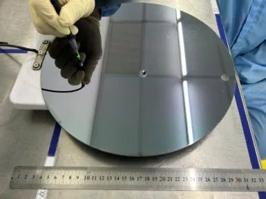
It is understood that AlN:GaN Short-Period Superlattice (SPSL) LED material is grown on a 6-inch sapphire substrate by plasma-assisted molecular beam epitaxy (PAMBE) technology (Figure 2). There is an artificial strain between this material and the underlying 400nm AlN buffer layer.

Figure 2:(a) Basic device structure of SPSL ultraviolet light emitting diode. (b)Transmission electron microscope image of the interface between recombination zone and chirped zone. (c)X-ray diffraction x-2h scan of SPSL grown on AlN buffer.
It can be seen from the figure that SPSL is composed of alternating GaN layers and AlN layers. By changing the thicknesses of these layers, the effective aluminum content of different Group III nitride materials can be obtained, thereby obtaining different LED target wavelengths. Using the SPSL structure reduces the resistivity by three times
The Silanna UV team tested the device. The device's 80nm/36-period recombination region and 450-nm bulk n-type region were separated by a 50-nm high-conductivity region. The high-conductivity region had a low aluminum content, which was a 1:4 single-layer GaN: Aluminum nitride, so the effective aluminum content during 37 cycles is 80%. Using the SPSL structure can reduce the resistivity by a factor of three, which is similar to the reported resistivity values for bulk Al0.8G0.2N materials. For wavelengths of 229-240 nm, the aluminum content in the recombination/large volume region is approximately 93-98%.
In addition, the final area of the device includes a 20-nanometer chirped/graded layer, which transitions to a 40-nanometer p-type GaN cap layer as the GaN layer thickness increases.
The research team said the purpose of the chirped layer is to improve hole injection from lower-bandgap GaN into the SPSL recombination region, and can also serve as an electron blocking layer to restrict electrons from crossing the recombination layer.
At the same time, the ionized acceptor concentration in the cap was measured to be approximately 1 x 10¹⁹/cm3, and the ionized donor concentration in the high-conductivity SPSL layer was estimated to be 8 x 10¹⁹/cm3. This material is made into passivated Mesa LEDs with titanium/aluminum contacts. Photoelectric measurements are made through a 2-inch integrating sphere at the bottom of the wafer. The wavelength and power performance of the device are uniform across the wafer. However, the electrical performance is not so uniform. The research team explained: This is because the series resistance and electrical characteristics are affected by etching and metallization processes, not just the MBE growth process.
It points out that a wafer with 233 1-nm wavelength devices can produce 10763 LEDs. The standard deviation of the wavelength at 4 inches inside the wafer is only 0.16 nanometers. At 20mA injection, the average optical power output of this inner part is 0.2 W. For devices more than half an inch from the edge of the wafer, the standard deviation of the drive voltage at 20 milliampe-hours is less than 0.16 volts.
The research team said that it is possible to produce areas larger than 4 inches with consistent performance. From the perspective of production volume and yield, the MBE growth SPSL LED method is one of the most promising methods.
Achieve the highest radiant flux of Far-C LED, with a light output of 17.4mW in 1A
The research team also packaged 1 mm x 1mm single crystal LEDs using the electrostatic discharge protection function of commercial Zener diode shunts. Before encapsulation with aluminum nitride ceramic material, the thickness of the LED was reduced to 275 m, and measurements were made in a 6-inch integrating sphere (Figure 3).

Figure 3:(a) Typical optical output power, wall insertion efficiency, and voltage vs. injection current for a device with a wavelength of 236nm. (b)According to the TM21 standard, a single device operates at a continuous current of 20mA for 3000 hours. (c)R70 percentile for 80 packaged devices.
Experiments show that a typical packaged device has a wall insertion efficiency of 0.55% at 50mA injection, a radiant flux of 1.7mW at a peak efficiency of 0.55%, and an optical output of 17.4mW at 1A. The research team stated that although this significantly exceeded the predetermined driving current, it was the highest radiation flux reported for extreme ultraviolet LEDs grown on sapphire substrates.
TAG:
Guess you want to see it
Popular information
-
With more than 75000 grains per time, British researchers developed Micro LED continuous roller tran
-
Zhejiang University's micro-level Micro-LED array achievements were selected into the top ten scient
-
Four Micro LED technologies achieve new progress
-
The JBD full-color Micro prototype has been shipped, but is it actually a stacked structure?
-
Domestic R &D team develops Micro LED high-efficiency backlight devices
-
99.88% yield! Seoul National University Micro LED Mass Transfer New Breakthrough
-
The latest research progress of ultraviolet LEDs comes from Sanan Optoelectronics
-
Many heavyweights in the academic community and industry jointly published an article on Micro LED r

-
Micro LED new breakthrough! Jingneng Optoelectronics's first 12-inch silicon substrate InGa-based tr
-
Reduced power consumption by 95%! Another Micro LED technology "refreshes" progress
the charts
- The best solution for AR glasses? Integrating Micro LEDs with advanced CMOS
- Red MicroLED R &D competition accelerates: Material innovation can solve the problem of luminous eff
- Micro LED heating capacity reduced by 40%! This study is supported by Samsung
- Zhejiang University's micro-level Micro-LED array achievements were selected into the top ten scient
- Red MicroLED R &D competition accelerates: Material innovation can solve the problem of luminous eff
- Analysis of huge transfer technology: How to break through the Micro LED display process problems?
- technology| Interpretation of MicroLED Technology in Mico Display Principles
- Micro LED achieves breakthrough results again
- Micro 0.4 released globally, opening a new era in the LED industry
- A team from Xiamen University designs artificial nanostructures that enhance deep ultraviolet light