technology| Interpretation of MicroLED Technology in Mico Display Principles
- author:
- 2024-05-27 09:35:58
microled technology based on Miro display principles is LED miniaturization and matrixing technology. Specifically, it is a high-density and minutely size LED array integrated on a single chip. Just as every pixel of an LED display can be addressed and can be driven individually to light, this can be regarded as a miniaturized version of an outdoor LED display, reducing the distance between pixels from millimeter level to micron level.
01
Micro LED Display Principle
The LED structure is designed to be thin, miniaturized, and arrayed, and the size is only about 1 - 10m; then the LEDs are transferred in batches to a circuit substrate (including lower electrodes and transistors), and the substrate can be on a hard and soft transparent or opaque substrate; and then the protective layer and upper electrodes are completed by using a physical deposition process, so that the upper substrate can be packaged and a Micro LED Display with a simple structure is completed.
02
Typical Micro LED structure
PN junction diode, composed of direct bandgap semiconductor material. When the upper and lower electrodes apply a forward bias to the LED, causing current to pass through, electrons and holes combine with the active region, emitting a single color light. mu; The full-width at half maximum FWHM of the main wavelength of the LED emission spectrum is only about 20nm, which can provide extremely high color saturation, usually greater than 120% NTSC.
Moreover, since 2008, the photoelectric conversion efficiency of LEDs has been greatly improved, and LEDs above 100 lm/W have become the standard for mass production. In the application of Micro LED Display, it has self-luminous display characteristics and a simple structure with almost no light-consuming elements, so it is easy to achieve low energy consumption (10% to 20% TFT-LCD energy consumption) or high brightness (more than 1000nits) display design. It can solve the two major problems in current display applications. First, more than 80% of the energy consumption of wearable devices, mobile phones, tablets and other devices lies in the display. Low-energy display technology can provide longer battery life; First, the problem is that the image on the display is whiter and the visibility becomes poor. High-brightness display technology can make its application scope wider.
03
Micro Display Principle
pixel structure
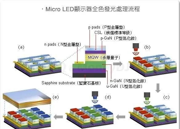
MicroLED displays generally use mature multi-quantum well LED chip technology. Taking a typical InGaN-based LED chip as an example, the MicroLED pixel unit structure is, from bottom to top, a sapphire substrate layer, a 25-nm GaN buffer layer, a 3-m N-type GaN layer, and an active layer including a multi-period quantum well (MQW)., a 0.25-m P-type GaN contact layer, a current spreading layer and a P-type electrode. When a forward bias voltage is applied to the pixel unit, holes in the P-type GaN contact layer and electrons in the N-type GaN layer both migrate to the active layer. Charge recombination occurs in the active layer, and energy is released in the form of luminescence after recombination.
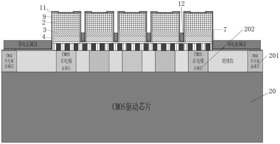
Compared with traditional LED displays, MicroLEDs have two major characteristics: one is miniaturization, and its pixel size and pixel spacing are reduced from millimeter to micron; the other is matrixing and integration. Its device structure includes LEDs prepared by CMOS process. Display driver circuit and LED matrix array.
array driving
Pixel cells of InGaN-based MicroLEDs are generally prepared through the following four steps. The first step is to etch the trench to the sapphire layer through an ICP etching process to isolate a separate strip GaN platform on the epitaxial wafer. The second step is to establish pixel cells of each specific size by ICP etching on the GaN platform. The third step is to prepare a Ni/Au current spreading layer on the P-type GaN contact layer through a lift-off process. The fourth step is to fabricate Ti/Au ohmic contact electrodes on the N-type GaN layer and the P-type GaN contact layer through thermal deposition. Among them, the cathodes of each column of pixels are connected through an N-type GaN layer common cathode, and the anodes of each row of pixels have different driving connection methods. The driving methods mainly include passive address drive (PM, also known as passive address drive), active address drive (AM, also known as active address drive) and semi-active address drive.
Among them, passive address driving is to make the pixel electrodes into a matrix structure. The anode (cathode) electrodes of each column (row) of pixels share a column (row) scan line, and the two layers of electrodes are electrically isolated by a deposited layer. The LED pixels located in the Xth and Yth rows are lit up by simultaneously gating the Xth and Yth columns, and each pixel is scanned dot by dot (or row by row) at high speed to realize the display mode of the entire screen.
In the active address driving mode, each Micro LED pixel has its corresponding independent driving circuit, and the driving current is provided by the driving transistor. The basic active matrix driving circuit is a dual-transistor single-capacitor circuit. In each pixel circuit, the gate transistor is used to control the switching of the pixel circuit, the driving transistor is connected with the power supply to provide stable current for the pixel, and the storage capacitor is used to store data signals. In order to improve display capabilities such as gray scale, complex active matrix driving circuits such as four-transistor dual capacitor circuits can be used.
The semi-active addressing driving method uses a single transistor as the driving circuit of Micro LED pixels, which can better avoid crosstalk between pixels. Semi-active driving performance is between active driving and passive driving because each column driving current signal requires separate modulation.
With the continuous advancement and development of technology, the application prospects of MicroLED technology in the display field will become more and more broad. In the future, it is expected to show its unique advantages in more scenes and bring people a more shocking and clear visual experience. Let us wait and see the continued innovation and breakthroughs of this technology.
TAG:
Guess you want to see it
Popular information
-
It can improve the light extraction rate of far-ultraviolet LEDs, and Silanna UV technology has beco
-
Red MicroLED R &D competition accelerates: Material innovation can solve the problem of luminous eff
-
Reduced power consumption by 95%! Another Micro LED technology "refreshes" progress
-
Major breakthroughs in MicroLED bandwidth and efficiency
-
Four Micro LED technologies achieve new progress
-
A team from Xiamen University designs artificial nanostructures that enhance deep ultraviolet light
-
Red MicroLED R &D competition accelerates: Material innovation can solve the problem of luminous eff

-
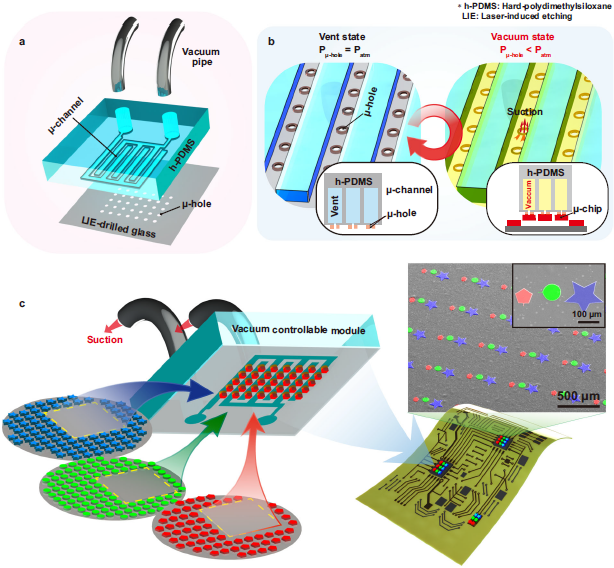
Zhejiang University's micro-level Micro-LED array achievements were selected into the top ten scient
-
Meta patent disclosed that enables high quantum efficiency Micro LED pixels
-
Domestic R &D team develops Micro LED high-efficiency backlight devices
the charts
- The best solution for AR glasses? Integrating Micro LEDs with advanced CMOS
- Red MicroLED R &D competition accelerates: Material innovation can solve the problem of luminous eff
- Micro LED heating capacity reduced by 40%! This study is supported by Samsung
- Zhejiang University's micro-level Micro-LED array achievements were selected into the top ten scient
- Red MicroLED R &D competition accelerates: Material innovation can solve the problem of luminous eff
- Analysis of huge transfer technology: How to break through the Micro LED display process problems?
- technology| Interpretation of MicroLED Technology in Mico Display Principles
- Micro LED achieves breakthrough results again
- Micro 0.4 released globally, opening a new era in the LED industry
- A team from Xiamen University designs artificial nanostructures that enhance deep ultraviolet light