Meta patent disclosed that enables high quantum efficiency Micro LED pixels
- author:
- 2024-06-07 13:30:39
Recently, Meta's patent called Semipolar micro-led was disclosed. In the patent, Meta describes a Micro LED pixel capable of achieving significant redshifts in the wavelength of emitted light and high quantum efficiency.
In view of the length of the full text, here only describes the high quantum efficiency achieved by Micro LED pixels. The original patent can be viewed in the U.S. Patent and Trademark Office.
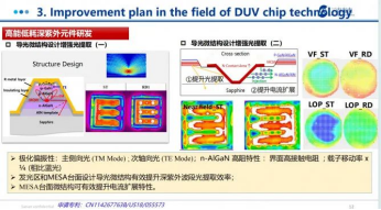
In the application of LEDs, the overall external quantum efficiency (EQE) plays a very critical position. It is mainly determined by the internal quantum efficiency (IQE) and the light extraction efficiency (LEE). It is used to characterize the performance of GaN-based Micro LEDs. An important parameter means how many electrically injected carriers can eventually be transformed into photons emitted by the device.
The Micro LEDs described by Meta can comprise a light-emitting layer grown on the semipolar surface of a pit structure formed in a doped semiconductor layer. The doped semiconductor layer can be etched by using a mask with sloped sidewalls and openings of a specific shape and orientation.
The doped semiconductor layer can encompass an n-doped GaN layer grown on a c-plane oriented substrate and can be etched to form a pit structure with facets tilted at an angle of approximately 50 to 75 relative to the c-plane. Therefore, each dimple structure may have an inverted pyramid shape, and the facets of the dimple structure may be semi-polar oriented. 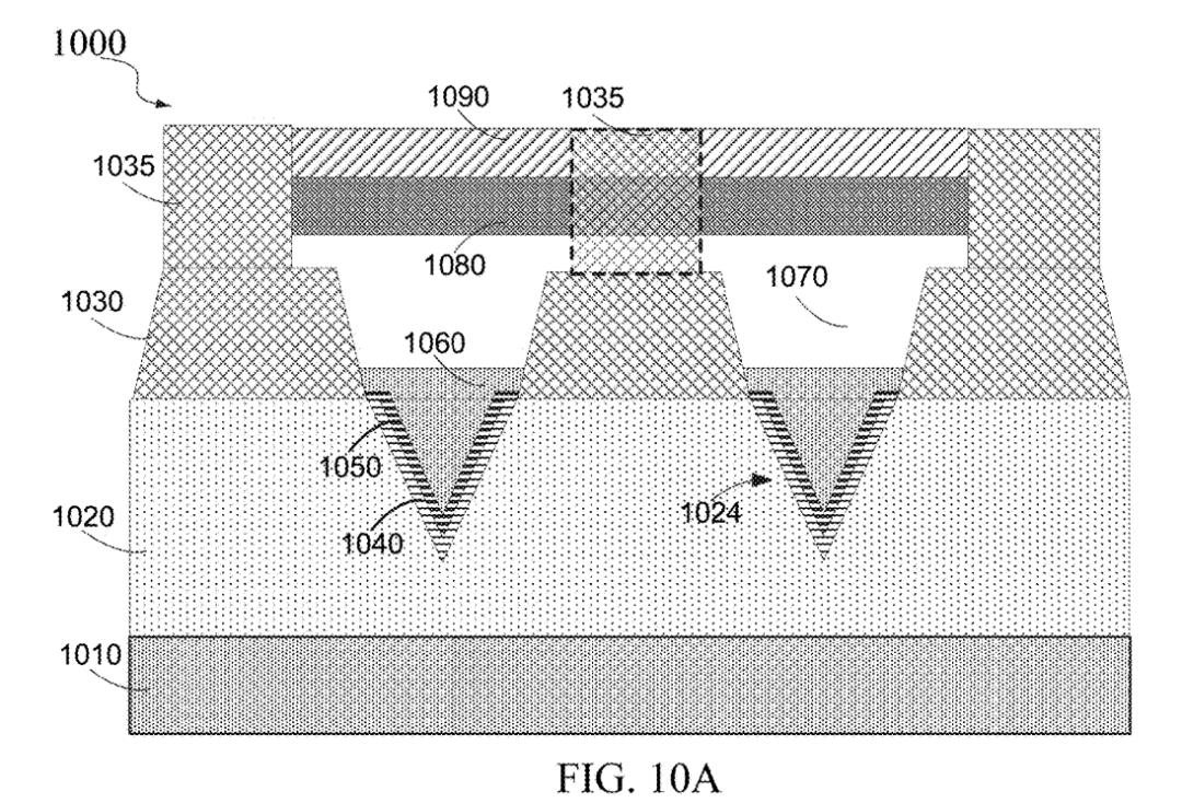
Meta patent disclosure can achieve high quantum efficiency Micro LED pixels.
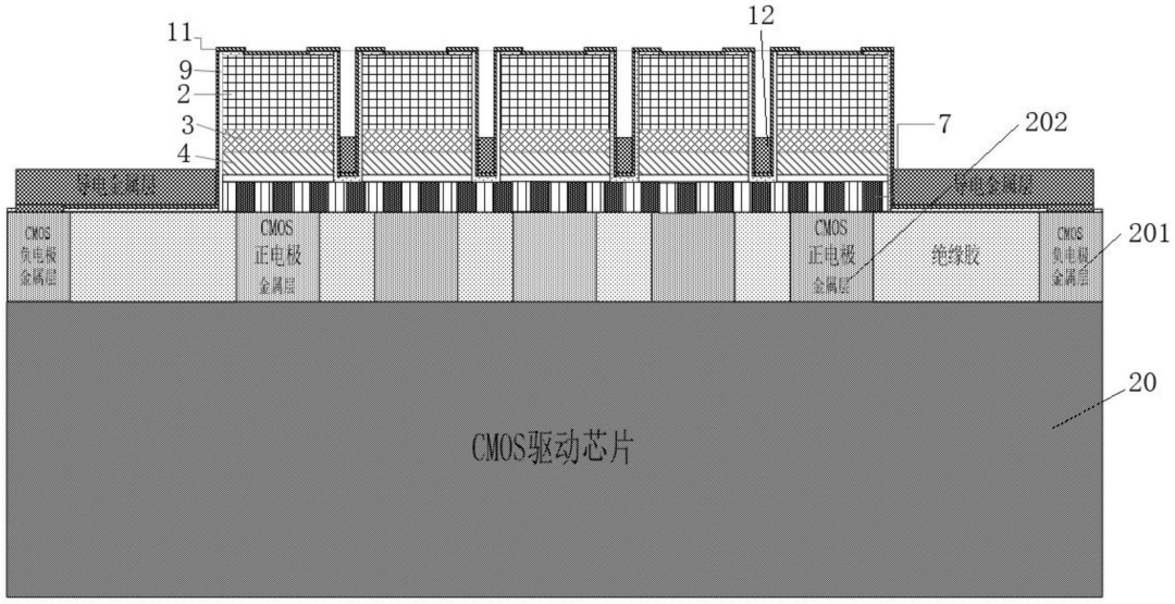
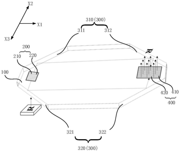
FIG. 10A shows an example of a micro LED pixel including a subpixel with a light-emitting layer formed on the semi-polar face of a recess formed in a layer of semiconductor material, in accordance with certain embodiments.
One or more quantum well layers (e.g., undoped GaN/InGaN layers) can be epitaxially grown on the semi-polar pit surface, an electron blocking layer (EBL) can be grown on the quantum well layer, and a p-doped GaN layer can be grown on the EBL layer and/or can fill the pit structure. Such Micro LED subpixels can be formed in each pit structure.
In one embodiment, a p-contact layer such as an indium tin oxide (ITO) layer and/or a metal layer may be formed on the p-doped GaN layer. The fabricated Micro LED chip with Micro LED subpixels formed in the pit structure can be bonded to the CMOS wafer through bond pads. Each bond pad may be larger than the size of the Micro LED sub-pixel, thereby allowing multiple Micro LED sub-pixels to be grouped into one Micro LED pixel.
TAG:
Guess you want to see it
Popular information
-
New progress in quantum dot patterning at Guangdong Academy of Sciences, suitable for Micro LEDs
-
Stanford University develops flexible, stretchable IC and successfully drives Micro LED screens
-
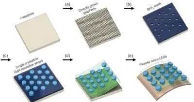
South Korean universities achieve growth of flexible GaN Micro LED arrays on graphene substrates
-
Micro 0.4 released globally, opening a new era in the LED industry
-
Meta patent disclosed that enables high quantum efficiency Micro LED pixels
-
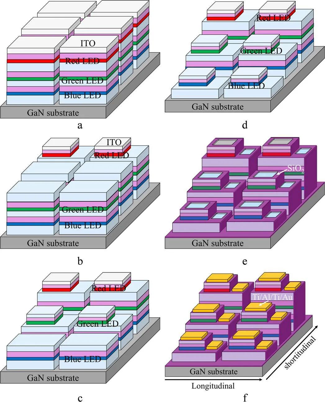
Researchers from the two universities collaborated to develop laminated full-color Micro LEDs
-
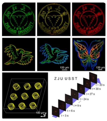
Zhejiang University's micro-level Micro-LED array achievements were selected into the top ten scient
-
Micro LED Innovation Breakthrough: The future of display technology has arrived
-
Or first for MicroLEDs! Fujian Institute of Paper Formosa develops efficient near-infrared quantum d
-
BOE and Peking University announced new patents involving AR displays and Micro LED chips
the charts
- The best solution for AR glasses? Integrating Micro LEDs with advanced CMOS
- Red MicroLED R &D competition accelerates: Material innovation can solve the problem of luminous eff
- Micro LED heating capacity reduced by 40%! This study is supported by Samsung
- Zhejiang University's micro-level Micro-LED array achievements were selected into the top ten scient
- Red MicroLED R &D competition accelerates: Material innovation can solve the problem of luminous eff
- Analysis of huge transfer technology: How to break through the Micro LED display process problems?
- technology| Interpretation of MicroLED Technology in Mico Display Principles
- Micro LED achieves breakthrough results again
- Micro 0.4 released globally, opening a new era in the LED industry
- A team from Xiamen University designs artificial nanostructures that enhance deep ultraviolet light