Analysis of huge transfer technology: How to break through the Micro LED display process problems?
- author:
- 2023-04-04 14:03:11
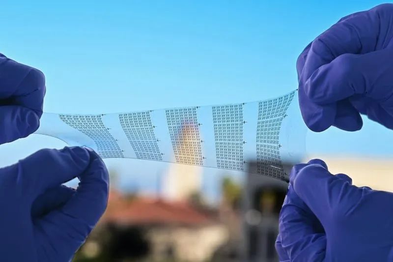
Compared with traditional LCDs and oleds, Micro LEDs have characteristics such as high resolution, low power consumption, high brightness, high contrast, high color saturation, fast response speed, thin thickness, and long life. They are considered to be the mainstream direction of future display technology., have extremely high application potential in VR/AR, high-definition, flexible, wearable and other display fields.
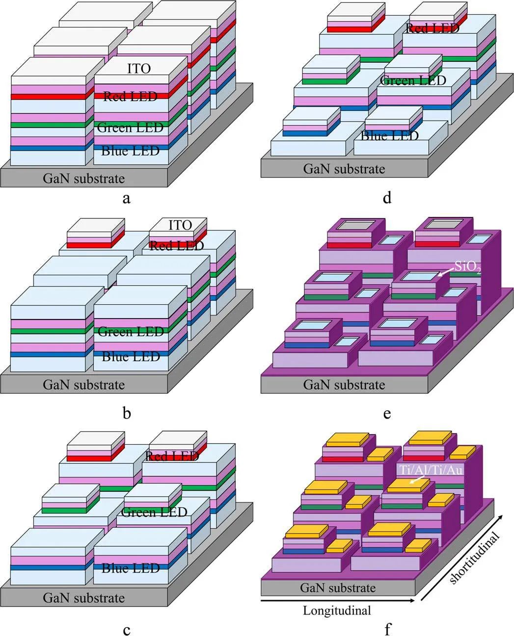
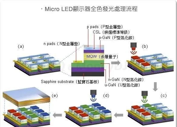
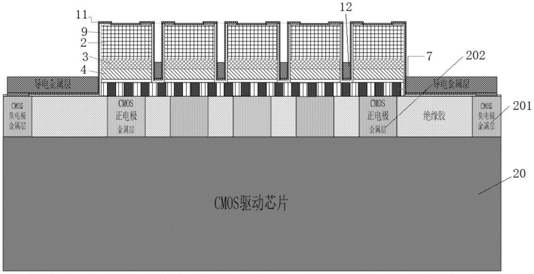
Micro LED displays are made up of millions of three-color RGB chips. Generally speaking, limited by epitaxial growth technology, it is extremely difficult to simultaneously grow high-quality three-color RGB chips on large-area epitaxial substrates. Therefore, it is necessary to grow millions or even tens of millions of micron three-color RGB chips grown on the epitaxial substrate. The chips are transferred to the driving circuit substrate in turn to achieve RGB arrangement.

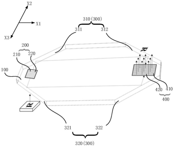
Schematic diagram of three-color RGB chip transfer
However, since the characteristic size of Micro LEDs is less than 100 m, it is difficult for traditional transfer technology to meet the requirements in terms of transfer efficiency and transfer accuracy. Traditional transfer technology has physical limits on the size requirements of a single chip. The chip is too small to transfer, and the transfer accuracy is difficult to meet; the robot arm also has time limits during the chip transfer process, and the transfer efficiency is difficult to improve, which means that traditional transfer technology and equipment are no longer suitable for the Micro LED transfer process.
Faced with the above technical challenges, in order to achieve rapid and accurate transfer and reduce subsequent maintenance pressure, a huge amount of transfer technology has emerged. Micro LED mass transfer technology has proven to be an effective solution to overcome the extreme requirements of assembling Micro LED chips. Micro LED massive transfer equipment uses laser transfer technology. It uses specially shaped square light spots and high-speed galvanometer scanning to achieve high-speed processing and transfer micron-sized Micro LED chips one by one to the underlying substrate (glass or film material). Micro LED massive transfer equipment is one of the core equipment in the Micro LED production process and is the key to affecting the yield and manufacturing cost of Micro LEDs.

Micro LED laser massive transfer technology schematic diagram
Since 2019, Han's Semiconductor has been deploying laser mass transfer technology to explore key solutions to meet the transfer requirements of Micro LED chips. In November 2021, it independently developed and launched the first solid-state Micro LED laser mass transfer equipment in China; In October 2022, it independently developed and launched the first excimer Micro LED laser mass transfer equipment in China, which passed the verification of head customers and achieved sales.
Micro LED laser massive transfer equipment

Equipment characteristics:
The shaped light spot is used to selectively transfer the chip to the lower substrate;
The chip is positioned accurately and without damage;
All transfers and transfers from any location can be realized.
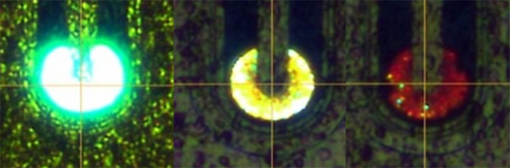
Processing effect:

Han's Semiconductor will continue to rely on its relatively comprehensive layout and integration capabilities to improve its core competitiveness for Micro LEDs and accelerate the pace of commercialization of Micro LEDs. In the future, Han's Semiconductor will continue to optimize its industrial layout and improve its own product structure, adhere to consistent high standards and strict requirements for product quality, continue to independently innovate development concepts, and make progress together and develop in a coordinated manner with the industry.
TAG:
Guess you want to see it
Popular information
-
Domestic R &D team develops Micro LED high-efficiency backlight devices
-
National Taiwan University teamed up with Yang Ming Jiao Tong University to make new progress in the
-
South Korean universities achieve growth of flexible GaN Micro LED arrays on graphene substrates
-
technology| Interpretation of MicroLED Technology in Mico Display Principles
-
It can improve the light extraction rate of far-ultraviolet LEDs, and Silanna UV technology has beco
-
Stanford University develops flexible, stretchable IC and successfully drives Micro LED screens
-
The best solution for AR glasses? Integrating Micro LEDs with advanced CMOS
-
Nanjing University team achieves all-nitride monolithic integration of Micro LEDs driven by quasi-ve
-
Analysis of the evolution path of Samsung Display XR Display's MicroLED microdisplay technology
-
The latest progress of Micro LED chips! 4 units disclosed
the charts
- The best solution for AR glasses? Integrating Micro LEDs with advanced CMOS
- Red MicroLED R &D competition accelerates: Material innovation can solve the problem of luminous eff
- Micro LED heating capacity reduced by 40%! This study is supported by Samsung
- Zhejiang University's micro-level Micro-LED array achievements were selected into the top ten scient
- Red MicroLED R &D competition accelerates: Material innovation can solve the problem of luminous eff
- Analysis of huge transfer technology: How to break through the Micro LED display process problems?
- technology| Interpretation of MicroLED Technology in Mico Display Principles
- Micro LED achieves breakthrough results again
- Micro 0.4 released globally, opening a new era in the LED industry
- A team from Xiamen University designs artificial nanostructures that enhance deep ultraviolet light