BOE and Peking University announced new patents involving AR displays and Micro LED chips
- author:
- 2024-06-04 14:54:07
Recently, BOE and Peking University have successively announced display-related patents, involving AR glasses products and the preparation of Micro LED chips.
BOE: A patent for an optical waveguide device and AR display device that improves light efficiency
According to information from the National Patent Office, Beijing BOE Technology Development Co., Ltd. has announced a patent for an optical waveguide device and AR display device. The application publication date is March 26, 2024, and the application publication number is CN117761825A. Patents can improve the light efficiency of AR display devices.

Photo source: National Patent Office
Patent information shows that the present disclosure provides an optical waveguide device and an AR display device. The optical waveguide device comprises: an optical waveguide plate, and a coupling-in grating, a reflective element and a coupling-out grating disposed on the optical waveguide plate; wherein the coupling-in grating is configured to couple incident light into the optical waveguide plate and form diffracted light in the optical waveguide plate; The reflective element is configured to receive the diffracted light from the optical waveguide plate and reflect the diffracted light to the coupling-out grating; and the coupling-out grating is configured to receive the diffracted light reflected from the reflective element and emit the diffracted light. The optical waveguide device and AR display device provided in embodiments of the present disclosure provide a new architecture for an AR augmented reality display system and can improve light efficiency.
It is reported that in the field of AR/VR equipment, BOE can provide Micro OLED display modules and Fast LCD modules. The size ranges from 0.39 inches to 5.5 inches. It has high resolution, fast response, high refresh rate and other characteristics, and can be applied to a variety of micro display scenarios. In addition, BOE's MLDE technology can also provide high-quality and high-reliability LED backlight products for display products in VR/AR and other fields.
Previously, BOE released a number of new micro display products, including the world's first 1.3-inch binocular 4K Micro oled display with a pixel density of 4000+PPI and a brightness of 5000nits. BOE has also launched an ultra-thin and large-viewing angle Si-OLED binocular optical system, which has high brightness and display density, while making the product thinner and thinner.
Peking University: Apply for a patent for Micro LED chips to reduce preparation complexity
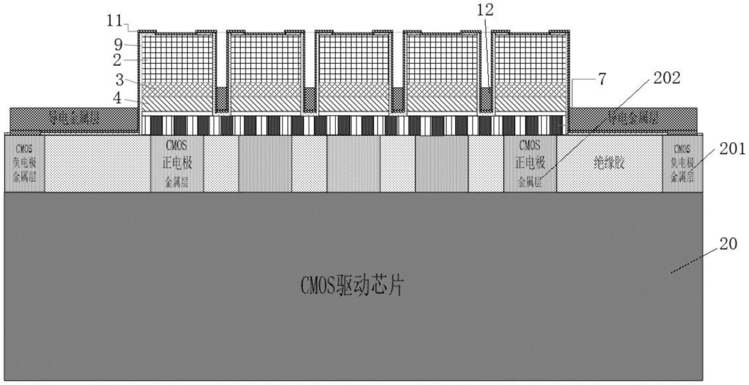
According to an announcement from the State Intellectual Property Office, Peking University applied for a preparation method for a Micro-LED chip array based on maskless secondary epitaxy, publication number CN117766642A, and the application date is December 2023. This patent reduces the complexity of the Micro LED preparation process.

Photo source: National Patent Office
The patent abstract shows that the present invention discloses a preparation method for Micro LED chip arrays based on maskless secondary epitaxy. The invention carries out dry etching on the GaN template to form a stress relaxed patterned GaN template, and then selects secondary epitaxial structures such as multiple quantum wells on the basis of the stress relaxed patterned GaN template, which effectively avoids dry etching on the multiple quantum well regions, thereby avoiding side wall etching damage of the multiple quantum wells; the stress relaxed patterned GaN template effectively relaxes the stress on n-type doped GaN; The compressive stress applied to the prestressed layer grown on the stress-relaxed patterned GaN template is partially relaxed, and the in-plane lattice constant is expanded, thereby reducing the energy required for indium incorporation and increasing the amount of indium in multiple quantum wells. Incorporation; The etching in preparing the stress-relaxed patterned GaN template makes only the top surface of the GaN micron pillar array a c-plane as a growth surface; selective secondary epitaxial growth does not require an additional mask, reducing the complexity of the Micro LED preparation process.
TAG:
Guess you want to see it
Popular information
-
The JBD full-color Micro prototype has been shipped, but is it actually a stacked structure?
-
Domestic R &D team develops Micro LED high-efficiency backlight devices
-
Micro LED Innovation Breakthrough: The future of display technology has arrived
-
Micro LED heating capacity reduced by 40%! This study is supported by Samsung
-
Red MicroLED R &D competition accelerates: Material innovation can solve the problem of luminous eff
-
The latest progress of Micro LED chips! 4 units disclosed
-
Huge transfer and breakthrough: 75,000 MicroLEDs can be transferred at a time
-
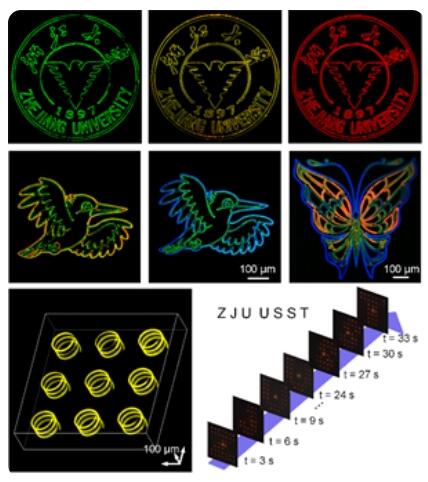
Zhejiang University's micro-level Micro-LED array achievements were selected into the top ten scient
-
With more than 75000 grains per time, British researchers developed Micro LED continuous roller tran
-
Nanjing University team achieves all-nitride monolithic integration of Micro LEDs driven by quasi-ve
the charts
- The best solution for AR glasses? Integrating Micro LEDs with advanced CMOS
- Red MicroLED R &D competition accelerates: Material innovation can solve the problem of luminous eff
- Micro LED heating capacity reduced by 40%! This study is supported by Samsung
- Zhejiang University's micro-level Micro-LED array achievements were selected into the top ten scient
- Red MicroLED R &D competition accelerates: Material innovation can solve the problem of luminous eff
- Analysis of huge transfer technology: How to break through the Micro LED display process problems?
- technology| Interpretation of MicroLED Technology in Mico Display Principles
- Micro LED achieves breakthrough results again
- Micro 0.4 released globally, opening a new era in the LED industry
- A team from Xiamen University designs artificial nanostructures that enhance deep ultraviolet light