Reduced power consumption by 95%! Another Micro LED technology "refreshes" progress
- author:
- 2024-06-04 15:54:24
According to South Korean media reports, the Korea Electronics and Telecommunications Research Institute (ETRI) has developed an advanced semiconductor chip packaging technology that can reduce semiconductor productionpower consumption by 95%.

ETRI researcher, source by ETRI
This new technology uses a new thin film material callednon-conductive thin film (NCF), developed by ETRI through its self-developed nanomaterial technology, made based on epoxy-based materials and reducing agents, and has a thickness range of10 to 20microns. This material has the high performance required for semiconductor packaging and can be used as a high-quality adhesive material.
In addition, ETRI develops packaging technology that can achieve high-precision processes, can be applied to various small chip packages, and can also be applied to the production of all high-end semiconductor products includingMicro LEDs.
It is worth noting that this accuracy can be achieved at room temperature, which is different from traditional methods that require heating to 100 ° C, resulting in higher power consumption, increased errors, and reduced reliability due to thermal expansion.
The ETRI research team revealed that severalMicro LED developers have participated in evaluating the new technology and achieved very positive preliminary test results. The new materialis expected to be commercially applied within three years, providing semiconductor display companies with low power consumption and environmentally friendly solutions.
In addition, the technology is expected to become a core material technology for manufacturing artificial intelligence semiconductors with high-performance requirements, such as semiconductors needed for autonomous driving and data centers.
It is reported that ETRI has also previously developed a SITRAB new material technology, which is the first technology to combine LED transfer and bonding processes into one.
TAG:
Guess you want to see it
Popular information
-
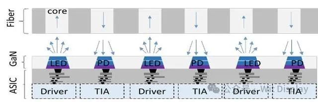
Many heavyweights in the academic community and industry jointly published an article on Micro LED r
-
technology| Interpretation of MicroLED Technology in Mico Display Principles
-
Or first for MicroLEDs! Fujian Institute of Paper Formosa develops efficient near-infrared quantum d
-
Apply materials to develop new Micro LED full-color technology
-
The latest progress of Micro LED chips! 4 units disclosed
-
BOE and Peking University announced new patents involving AR displays and Micro LED chips
-
With more than 75000 grains per time, British researchers developed Micro LED continuous roller tran
-
Analysis of the evolution path of Samsung Display XR Display's MicroLED microdisplay technology
-
Micro 0.4 released globally, opening a new era in the LED industry
-
Huge transfer and breakthrough: 75,000 MicroLEDs can be transferred at a time
the charts
- The best solution for AR glasses? Integrating Micro LEDs with advanced CMOS
- Red MicroLED R &D competition accelerates: Material innovation can solve the problem of luminous eff
- Micro LED heating capacity reduced by 40%! This study is supported by Samsung
- Zhejiang University's micro-level Micro-LED array achievements were selected into the top ten scient
- Red MicroLED R &D competition accelerates: Material innovation can solve the problem of luminous eff
- Analysis of huge transfer technology: How to break through the Micro LED display process problems?
- technology| Interpretation of MicroLED Technology in Mico Display Principles
- Micro LED achieves breakthrough results again
- Micro 0.4 released globally, opening a new era in the LED industry
- A team from Xiamen University designs artificial nanostructures that enhance deep ultraviolet light