New progress in quantum dot patterning at Guangdong Academy of Sciences, suitable for Micro LEDs
- author:
- 2024-06-04 15:00:33
In recent years, with the rapid development of communication technology and people's pursuit of display color and practicality, display technology has shown diversified development. Quantum dots have attracted widespread attention as a light-conversion material with great advantages in color purity, brightness, color gamut, quantum efficiency, etc. When using a light-conversion layer prepared based on quantum dots and efficient blue active light-emitting devices When combined to achieve full-color display, it will be very helpful to solve the challenges faced by new display technologies such as oled and Micro LED.
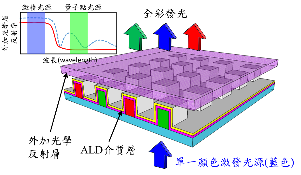
In the above-mentioned light conversion applications, red and green light quantum dots must correspond one-to-one to the corresponding blue light pixels to achieve the purpose of full-color display. Therefore, appropriate micro-nano processing technology needs to be developed to integrate quantum dots into pixels. However, the existing quantum dot patterning technology still poses certain challenges for preparing high-thickness and high-resolution quantum dot light-conversion films. Therefore, the new display team of the Institute of Semiconductor has carried out research and development of universal quantum dot patterning technology. A series of innovative research.
Recently, researchers at the Institute of Semiconductors of the Guangdong Province Academy of Sciences have developed a simple and compatible patterning method to prepare quantum dot photoconversion films with a thickness of more than 10 m. This method combines the advantages of replication, plasma etching and transfer. The advantages of the three processes are referred to as RM-PE-TP patterning technology for short. The specific process flow is shown in Figure 1. The quantum dot polymer materials used in this technology are simple and easily available to prepare, which well avoids the problems of complex quantum dot surface modification and material composition necessary in other patterning methods.

Figure 1: Process flow chart of RM-PE-TP patterning technology
In addition, the replication process is very conducive to obtaining quantum dot films with a thickness of more than 10 m, and the resolution and thickness of the quantum dot array are easy to adjust. In general, the entire patterning method has basically no damage to the optical properties of the quantum dot material, which facilitates the integration of polychromatic quantum dot patterning, and even further improves the resolution of the quantum dot pattern through monochromatic integration.
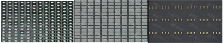
Therefore, based on the above-mentioned RM-PE-TP patterning technology, the research team finally prepared a patterned quantum dot polymer film with a resolution of up to 669 ppi and a film thickness of up to 19.74 m, and obtained a large area on a flexible substrate. The high-resolution quantum dot thick film shows that this technology has great application potential in large-scale flexible quantum dot patterning integration.

Figure 2: Quantum dot films prepared based on RM-PE-TP patterning method
In addition, the team also initially verified the feasibility of simply integrating the above-mentioned quantum dot polymer film as a light conversion layer into blue Micro LED devices to achieve light conversion applications, and found that increasing the thickness of the quantum dot film can improve the light conversion efficiency. The related research results, titled Wafer-scale patterning of high-resolution quantum dot films with a thickness over 10 m for improved color conversion, were published in the journal Nanoscale.
The research work is supported by projects such as the National Natural Science Foundation of China, the National Key Research Plan, the Action Fund Project of the Comprehensive Industrial Technology Innovation Center of the Provincial Academy of Sciences, and the Major Special Fund of Guangdong Province. Dr. Zou Shenghan from the new display team of the Institute of Semiconductor is the lead author, and Professor Gong Zheng, the subject leader, is the corresponding author.
TAG:
Guess you want to see it
Popular information
-
Nanjing University team achieves all-nitride monolithic integration of Micro LEDs driven by quasi-ve
-
Red MicroLED R &D competition accelerates: Material innovation can solve the problem of luminous eff
-
Meta patent disclosed that enables high quantum efficiency Micro LED pixels
-
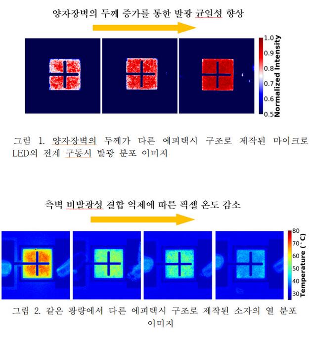
Micro LED heating capacity reduced by 40%! This study is supported by Samsung
-
The best solution for AR glasses? Integrating Micro LEDs with advanced CMOS
-
Huge transfer and breakthrough: 75,000 MicroLEDs can be transferred at a time
-
99.88% yield! Seoul National University Micro LED Mass Transfer New Breakthrough
-
Micro LED Innovation Breakthrough: The future of display technology has arrived
-
Analysis of huge transfer technology: How to break through the Micro LED display process problems?
-
Domestic R &D team develops Micro LED high-efficiency backlight devices
the charts
- The best solution for AR glasses? Integrating Micro LEDs with advanced CMOS
- Red MicroLED R &D competition accelerates: Material innovation can solve the problem of luminous eff
- Micro LED heating capacity reduced by 40%! This study is supported by Samsung
- Zhejiang University's micro-level Micro-LED array achievements were selected into the top ten scient
- Red MicroLED R &D competition accelerates: Material innovation can solve the problem of luminous eff
- Analysis of huge transfer technology: How to break through the Micro LED display process problems?
- technology| Interpretation of MicroLED Technology in Mico Display Principles
- Micro LED achieves breakthrough results again
- Micro 0.4 released globally, opening a new era in the LED industry
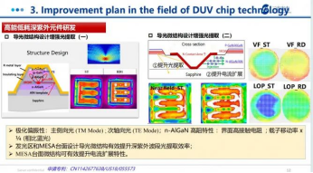
- A team from Xiamen University designs artificial nanostructures that enhance deep ultraviolet light