The latest research progress of ultraviolet LEDs comes from Sanan Optoelectronics
- author:
- 2024-06-04 14:59:26
Recently, Zang Yashu, manager of the chip development department and director of the process department of Xiamen San 'an Optoelectronics Co., Ltd., gave a keynote report on the current status and technical challenges of solid-state ultraviolet (UVA/B/C) light sources, and shared the latest research progress.
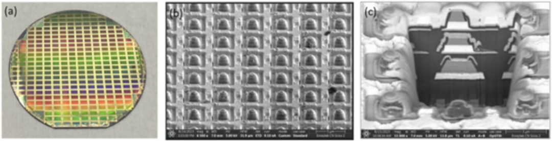
The wavelength of the ultraviolet LED light source ranges from 250nm to 420nm, spanning the three ultraviolet bands of UVA, UVB, and UVC. Although ultraviolet solid-state light sources have been widely used in industry and consumer electronics, ultraviolet LED light sources in different wavelength bands still face different technical challenges in large-scale production. Light source devices in the UVA band can currently achieve high electro-optical conversion efficiency and have successfully replaced mercury lamp light sources as the first choice in application fields such as photocuring and photocatalytic. However, the electro-optical efficiency of UVA solid-state light sources still has greater room for improvement. For LED devices in the UVB and UVC bands, as the Al component content of quantum structures increases, the preparation of materials with high crystal quality and high stability is becoming more and more challenging.

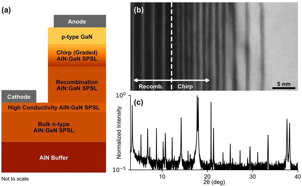
At the same time, how to reduce self-absorption and break through light extraction efficiency in UVC band deep ultraviolet LED devices is also the key to improving WPE. In its research work, the focus is on high-crystal-quality AlxGa1-xN epitaxial technology, which reduces defects and stresses in quantum structures by using NPSS and superlattice insertion layers for measurements; and innovatively introduces highly reflective electrode systems to improve LED devices. Photon extraction efficiency, thus promoting a breakthrough in performance of the entire ultraviolet (UVA/B/C) product line.

The report details the improvement plans in the field of UVA chip technology, the improvement plans in the field of DUV chip technology, and the latest developments in the ultraviolet product and application market, covering the progress of the 385/395 nm band product technology stage, the progress of the 365 nm band product technology stage, and the progress of DUV product technology stage, the underlying AlN quality improves material defect density, AlN Void Structure enhances light extraction, and the development of high-energy and low-consumption deep ultraviolet components. Among them, in the research on the formation mechanism of ohmic contacts in the n-Ga(Al)N electrode system in the development of high-energy and low-consumption deep ultraviolet components, when n-type high-Al-composition AlGaN and traditional Ti-based metal electrodes are annealed at high temperatures, TiN islands are easy to form at the interface. Au diffuses into the AlGaN material along the surface of the TiN island to form AuGa compounds, which in turn forms voids at the gold-half interface and reduces the flatness of the metal electrode film layer. Designing an n-type electrode structure to optimize fusion conditions can effectively improve flatness and reduce contact resistance. Explore high-efficiency chip stack structures to solve the problem of low carrier mobility caused by difficult doping of AlGaN with high Al composition; optimize the n hole size r and the n to n distance d to achieve the lowest n-type contact impedance and the best expansion current, and achieve a ~17% improvement in WPE.
TAG:
Guess you want to see it
Popular information
-
Domestic R &D team develops Micro LED high-efficiency backlight devices
-
It can improve the light extraction rate of far-ultraviolet LEDs, and Silanna UV technology has beco
-
Many heavyweights in the academic community and industry jointly published an article on Micro LED r
-
New progress in quantum dot patterning at Guangdong Academy of Sciences, suitable for Micro LEDs
-
Micro LED Innovation Breakthrough: The future of display technology has arrived
-
Micro LED new breakthrough! Jingneng Optoelectronics's first 12-inch silicon substrate InGa-based tr
-
The latest progress of Micro LED chips! 4 units disclosed
-
Nanjing University team achieves all-nitride monolithic integration of Micro LEDs driven by quasi-ve
-
Major breakthroughs in MicroLED bandwidth and efficiency
-
The JBD full-color Micro prototype has been shipped, but is it actually a stacked structure?
the charts
- The best solution for AR glasses? Integrating Micro LEDs with advanced CMOS
- Red MicroLED R &D competition accelerates: Material innovation can solve the problem of luminous eff
- Micro LED heating capacity reduced by 40%! This study is supported by Samsung
- Zhejiang University's micro-level Micro-LED array achievements were selected into the top ten scient
- Red MicroLED R &D competition accelerates: Material innovation can solve the problem of luminous eff
- Analysis of huge transfer technology: How to break through the Micro LED display process problems?
- technology| Interpretation of MicroLED Technology in Mico Display Principles
- Micro LED achieves breakthrough results again
- Micro 0.4 released globally, opening a new era in the LED industry
- A team from Xiamen University designs artificial nanostructures that enhance deep ultraviolet light