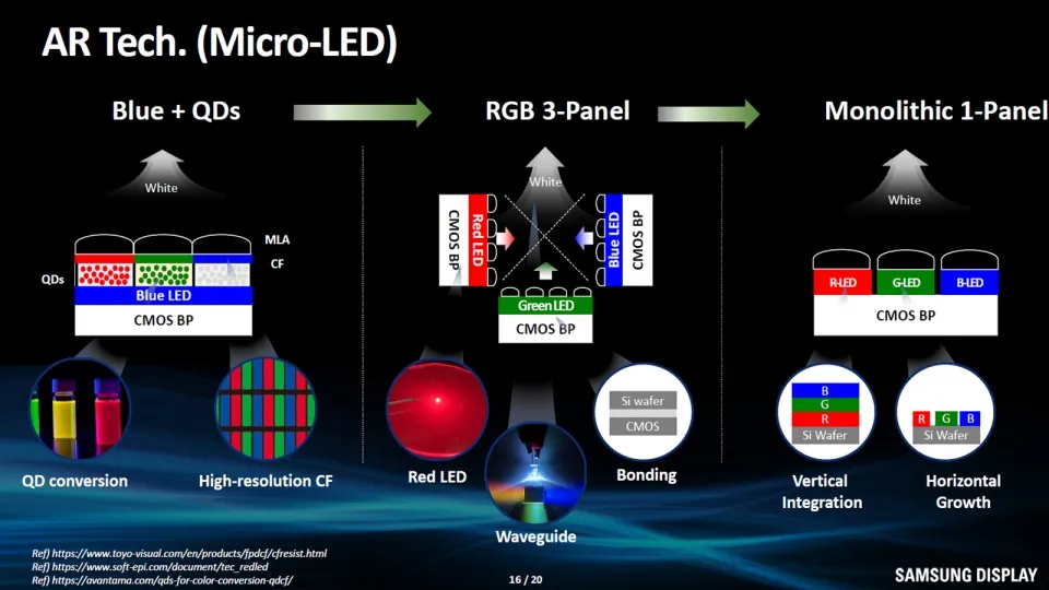
Nanjing University team achieves all-nitride monolithic integration of Micro LEDs driven by quasi-ve
- author:
- 2024-06-06 09:04:52
GaN-based Micro-LEDs are considered to be the most promising next-generation display technology after LCD and oled due to their advantages such as high brightness, high stability, long life and low power consumption. In display applications, it is often necessary to integrate the driving circuit and the Micro-LED through heterogenous integration to achieve the purpose of controlling a single pixel. Studying a more efficient and reliable integration method of Micro-LED and the driving circuit is of great significance to display applications.
Recently, the team of Zhuang Zhe and Liu Bin of Nanjing University proposed an all-nitride monolithic integration method driven by quasi-vertical MOSFETs for GaN-based Micro-LEDs, which enabled current driving of Micro-LED chips of different size. Related research work was recently published in IEEE Electron Device Letters titled Monolithic integration of GaN-based green micro-LEDs and quasi-vertical MOSFETs utilizing a hybrid tunnel junction.

Figure (a) Schematic diagram of GaN Micro-LED/MOSFET integrated device. Figure (b) Output curve of a 130 m diameter MOSFET. Figure (c) Light emission diagram of a 60-m-diameter Micro-LED/MOSFET integrated unit under different gate voltages. Figure (d) IV and LOP characteristics of a 60-m-diameter Micro-LED/MOSFET integrated cell at different gate voltages.
research highlights
The homogeneous integration of GaN-based Micro-LEDs and their drivers (such as HEMTs, MOSFETs, etc.) can give full play to the advantages of GaN materials and obtain a Micro-LED integrated unit with faster switching speed, higher temperature and voltage resistance, and higher efficiency. It has shown huge application prospects in Micro-LED transparent displays, flexible displays and visible light communications. However, most homogeneous integrations require selective epitaxial growth or precise control of etch depth, which greatly increases the difficulty and cost of preparation.
The research team of Nanjing University used MBE to secondarily grow a high-quality tunnel junction structure on commercial LED epitaxial wafers. On the one hand, the tunnel junction serves as a current extension layer for Micro-LEDs, and on the other hand, it can form a quasi-vertical npn type MOSFET with p-n junction LEDs. During the preparation process, only one etching step is needed to define the light-emitting area of the Micro-LED and the channel length of the MOSFET at the same time, and the homogeneous integration of the Micro-LED and the quasi-vertical MOSFET is achieved through n-type GaN lateral connection. GaN-based MOSFETs have similar current driving capabilities to oxide thin film transistors, and the overall integration scheme is less difficult to prepare and is easily compatible with existing chip structures and preparation processes. For a 60-m-diameter Micro-LED /MOSFET integrated unit, when the gate voltage of the MOSFET is 16V and the anode voltage of the Micro-LED is 5 V, the current flowing through the Micro-LED reaches 0.3 mA (10 A/cm2), and its output optical power reaches 0.12 mW (4.2 W/cm2), which can fully meet the Micro-LED display requirements. This research provides a new technical path for the future application of all-nitride optoelectronic integration in flexible Micro-LED displays, transparent displays, and visible light communications.
Paper information
Sang Yimeng, a doctoral student at the School of Electronic Science and Engineering of Nanjing University, is the first author of the article, and doctoral student Zhang Dongqi also made important contributions to this article. Assistant Professor Zhuang Zhe, School of Integrated Circuits, Nanjing University, and Professor Liu Bin, School of Electronic Science and Engineering, are co-corresponding authors of this article. Professor Zhang Rong, Professor Wang Xinran, Professor Wang Ke and Associate Professor Tao of Nanjing University provided in-depth guidance on the epitaxial growth and device technology of this work.
This work has been funded by fund projects such as the National Key Research and Development Plan, the National Natural Science Foundation of China, the Frontier Technology Plan of the Natural Science Foundation of China, the Natural Science Foundation of Jiangsu Province, and the Central University Basic Research Fund. At the same time, this work was supported by the School of Electronic Science and Engineering of Nanjing University, the Key Laboratory of Advanced Optoelectronic Materials of Jiangsu Province and the Micro Manufacturing and Integrated Process Center of Nanjing University.
TAG:
Guess you want to see it
Popular information
-
The latest research progress of ultraviolet LEDs comes from Sanan Optoelectronics
-
Analysis of the evolution path of Samsung Display XR Display's MicroLED microdisplay technology
-
Four Micro LED technologies achieve new progress
-
99.88% yield! Seoul National University Micro LED Mass Transfer New Breakthrough
-
Analysis of huge transfer technology: How to break through the Micro LED display process problems?
-
Reduced power consumption by 95%! Another Micro LED technology "refreshes" progress
-
With more than 75000 grains per time, British researchers developed Micro LED continuous roller tran
-
technology| Interpretation of MicroLED Technology in Mico Display Principles
-
The best solution for AR glasses? Integrating Micro LEDs with advanced CMOS
-
A team from Xiamen University designs artificial nanostructures that enhance deep ultraviolet light
the charts
- The best solution for AR glasses? Integrating Micro LEDs with advanced CMOS
- Red MicroLED R &D competition accelerates: Material innovation can solve the problem of luminous eff
- Micro LED heating capacity reduced by 40%! This study is supported by Samsung
- Zhejiang University's micro-level Micro-LED array achievements were selected into the top ten scient
- Red MicroLED R &D competition accelerates: Material innovation can solve the problem of luminous eff
- Analysis of huge transfer technology: How to break through the Micro LED display process problems?
- technology| Interpretation of MicroLED Technology in Mico Display Principles
- Micro LED achieves breakthrough results again
- Micro 0.4 released globally, opening a new era in the LED industry
- A team from Xiamen University designs artificial nanostructures that enhance deep ultraviolet light