Red MicroLED R &D competition accelerates: Material innovation can solve the problem of luminous eff
- author:
- 2023-04-03 10:51:53
CINNO Research Industry Information, as we all know, making high-brightness red Micro-LED chips for augmented reality and virtual reality devices has always been full of difficulties. Now Kubos Semiconductor has proposed a little-known material and believes it can solve this problem.
As major technology giants rushed to launch a variety of AR and VR devices to provide users with the vivid and bright images they had been waiting for, they all finally encountered such a common bottleneck: the development of red Micro-LED chips. Since inherent defects in materials can have serious effects when the device size is very small, the luminous efficiency of all LEDs currently decreases as the device size decreases, among which red LEDs are particularly obvious.
According to foreign media eetimes, recently, UK-based startup Kubos Semiconductor proposed a solution that they believe can solve this problem well. quot; The development of red Micro-LED chips has always kept people awake at night because no one can make traditional gallium nitride materials used in blue and green LED device manufacturing work effectively in longer red bands. Caroline O'Brien, CEO of Kubos Semiconductor, said: If you want to find a breakthrough, you have to look at this issue in a different way, and this is what we have been doing. quot;
So, what problems have we encountered in the development of red Micro-LED chips? The practical problem is that if a typical blue LED is reduced from the current common size to 5 microns, its luminous efficiency will drop sharply from about 90% to about 40%. Although there has been a large decline, it is already acceptable from an application perspective. Similarly, for red LEDs, their luminous efficiency will drop sharply from 60% to about 1%. Such a large decline is the crux of the current problem, and the main reason for this difference is the materials used to make these devices. different.
To date, blue and green LEDs have typically been made of indium gallium nitride (InGaN) materials. However, when developers also use InGaN materials to make longer-wavelength red LED devices, subtle differences in material composition will produce a strong polarization field in the light-emitting area of the device, which greatly reduces the light-emitting efficiency. As a result, most device manufacturers have begun to choose to use indium gallium phosphide (InGaP) semiconductor materials to make red LED devices. This approach was effective until problems with Micro-LED applications and their expansion emerged.
Some of the most intelligent people in the industry have been trying to find solutions from existing Micro-LED material systems. Blue laser diode pioneer and Nobel Prize winner Shuji Nakamura and colleagues at the University of California, Santa Barbara are moving in this direction to improve red Micro-LED chips made of InGaN and InGaP materials by minimizing defect effects. Zhe Zhuang and colleagues at King Abdullah University of Science and Technology (KAUST) in Saudi Arabia are using a new chemical treatment to improve the luminous efficiency of the red Micro-LEDs they developed based on GaN materials.
In fact, start-ups around the world are currently focusing on the manufacturing of red Micro-LEDs. South Korean ultraviolet LED manufacturer Soft Epi is improving the luminous efficiency of GaN-based red Micro-LEDs by adjusting growth processes. Micledi, a derivative company based in Imec, Belgium, recently announced the successful launch of an AlInGaP Micro-LED chip that emits Ferrari red light. In the UK, Porotech, a spin-off startup at the University of Cambridge, has developed porous GaN wafers, which they call PoroGaN, and believe will be the basis for manufacturing Micro-LED chips that emit light in various colors. In addition, Porotech recently teamed up with Wales-based compound semiconductor wafer supplier IQE to develop wafer products.
However, amid this increasingly active technology development activity, Kubos Semiconductor still insists that the universal materials system is the ultimate way forward for blue, green and red Micro-LEDs. For executives at the startup, this material that could win future victories is another GaN.
take different approaches
Although the industry's love for GaN is mainly focused on alloys with hexagonal crystal structures, David Wallis, founder of Kubos Semiconductor, also from Cardiff University and Cambridge University, has been studying a type of cubic GaN for many years. Because cubic GaN has higher crystal symmetry, this GaN variant can be unaffected by the strong polarization field, which, as mentioned above, reduces the luminous efficiency of GaN-based red LEDs.
So why is everyone concerned about GaN with a hexagonal crystal structure? In fact, as early as the 1990s, research on the growth of cubic GaN began to stall because the material may be thermodynamically unstable, making it difficult to grow the material with high quality on most substrates. At about the same time, research on the growth of hexagonal GaN became hot, and as the pace of device development accelerated, most researchers slowly began to forget about cubic GaN.
However, Wallis and his colleagues insisted on growing cubic GaN on a wafer with a thin SiC substrate. Anvil Semiconductor, a subsidiary of the University of Warwick in the United Kingdom, was the first to design silicon-based SiC substrates for developers of SiC power electronic devices. Later, Wallis and his team successfully developed a stable process for growing cubic GaN on the above substrate, and based on this achievement, Kubos Semiconductor Company was established. Since then, the company has been producing 150-mm wafers using the industry-standard metal-organic chemical vapor deposition (MOCVD) process to grow cubic GaN.

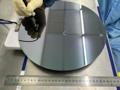
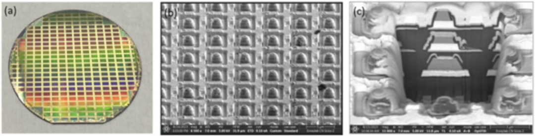
Figure 1. 150 mm GaN LED wafer passed wafer probe testing (Photo source: Kubos Semiconductor)
"Silicon substrates can be compatible with CMOS processes, and due to the low lattice mismatch between thin SiC layers and cubic GaN, we can force the growth of GaN into a cubic state, O'Brien said: With the commercialization of SiC power devices, the cost of this SiC layer will be significantly reduced, which will allow our complete solution to begin to compete with current Micro-LED manufacturing methods that use quantum dots or grow GaN on sapphire substrates.& quot;
Kubos plans to grow cubic GaN on larger 200-mm silicon carbide wafers, which, according to O'Brien, is the real best cost point"
Caroline O'Brien, CEO of Kubos, believes that the countless patents accumulated around its cubic GaN process have given the company a very large commercial advantage. In addition, she also pointed out that currently only a few players in the industry are studying cubic gallium nitride, such as the University of Illinois at Urbana-Champaign and Rensselaer Institute of Technology in the United States and the University of Paderborn in Germany. Moreover, these research institutions have not yet developed commercial devices.
O'Brien said: Cubic GaN has opened up a whole new world, a relatively untapped space compared to the IP minefield where hexagonal GaN is grown. quot;
Kubos recently manufactured a 50-micron diameter cubic GaN unpackaged Micro-LED chip that can emit red light. They hope to prove that it is possible to make longer-wavelength Micro-LEDs using cubic GaN solutions. Currently, the company is increasing its wafer supply to support customers in customizing its proprietary red Micro-LED chips. O'Brien estimates that the external quantum efficiency of these initial LED devices is about 3%.

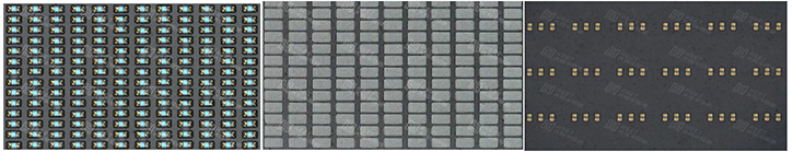
Figure 2. Green, amber and red Micro-LED devices with diameters of 50 microns made by Kubos Semiconductor. They are currently working to improve the luminous efficiency of red LED structures (Source: Kubos Semiconductor)
O'Brien said: A luminous efficiency goal close to 20% is achievable in the future, when this Micro-LED technology will become very meaningful in extending battery life, and I believe this goal will be achieved in the next five years.& quot;
For technology giants that are working hard to produce high-resolution, high-brightness AR/VR smart glasses, this technology and light-emitting devices will undoubtedly be very good news. At the same time, it will also allow Kubos Semiconductor to gain more and more benefits in the future. Many companies favor and even invite them to acquire them.
Finally, O'Brien said her goals include seeing the technology used in a variety of products, including traditional LED lighting, communications and Micro-LEDs. But I do think we are likely to be acquired because of the underlying nature of our industry.& quot;
TAG:
Guess you want to see it
Popular information
-
Micro LED new breakthrough! Jingneng Optoelectronics's first 12-inch silicon substrate InGa-based tr
-
The latest progress of Micro LED chips! 4 units disclosed
-
Four Micro LED technologies achieve new progress
-
Micro LED achieves breakthrough results again

-
Micro LED Innovation Breakthrough: The future of display technology has arrived
-
Red MicroLED R &D competition accelerates: Material innovation can solve the problem of luminous eff
-
Nanjing University team achieves all-nitride monolithic integration of Micro LEDs driven by quasi-ve
-
Domestic R &D team develops Micro LED high-efficiency backlight devices
-
Huge transfer and breakthrough: 75,000 MicroLEDs can be transferred at a time
-
The JBD full-color Micro prototype has been shipped, but is it actually a stacked structure?
the charts
- The best solution for AR glasses? Integrating Micro LEDs with advanced CMOS
- Red MicroLED R &D competition accelerates: Material innovation can solve the problem of luminous eff
- Micro LED heating capacity reduced by 40%! This study is supported by Samsung
- Zhejiang University's micro-level Micro-LED array achievements were selected into the top ten scient
- Red MicroLED R &D competition accelerates: Material innovation can solve the problem of luminous eff
- Analysis of huge transfer technology: How to break through the Micro LED display process problems?
- technology| Interpretation of MicroLED Technology in Mico Display Principles
- Micro LED achieves breakthrough results again
- Micro 0.4 released globally, opening a new era in the LED industry
- A team from Xiamen University designs artificial nanostructures that enhance deep ultraviolet light