National Taiwan University teamed up with Yang Ming Jiao Tong University to make new progress in the
- author:
- 2024-06-04 16:38:20
With the vigorous development of smart wearable devices and the widespread spread of the Internet, we are seeing the advent of an era of Internet of Things. In this context, any connected device requires a smart display to enhance interaction with users. To be able to meet the conditions of this environment, we must have a display device that is power-saving, high-efficiency, fast response, full-color, and small in size.
At present, under the attention of industry, academia and research circles, many novel technologies have been developed and put into the module prototype display of this smart display device. Including traditional liquid crystals or Organic LEDs (oleds), preliminary products have been developed under the strong promotion of relevant manufacturers. In the other direction, micro light emitting diodes (Micro LEDs) are used to fabricate micro displays.
Due to the requirements for display size and pixel size and resolution, we must develop a high-efficiency light-emitting element as a pixel, and this pixel must also have full-color functions. In past technologies, existing assembly technologies can often be used, such as pick and place, which can be used on the large-area outdoor LED display screens currently seen. But once the component size is reduced to less than five microns, many existing assembly techniques become impractical.
At the same time, the external quantum efficiency of the device will also drop significantly due to the increased recombination of non-radiative carriers and the relatively large sidewall area [1, 2], resulting in a significant increase in the power consumption of the overall module. To solve this problem, we must make fundamental changes to the overall module architecture.
One such method is to introduce the concept of a color conversion layer. The color conversion layer uses high-energy photons to excite lower-energy visible light photons (usually red and green) to achieve the effect of a full-color screen. However, how to combine color conversion levels onto a micro-LED matrix is still a topic of academic research.

Fig. 1 Schematic diagram of high-efficiency color conversion layer. Among them, the purple layer is an additional optical reflective layer. The top left is a schematic diagram of the reflectivity of a traditional DBR mirror (dotted line) and the redesigned optical mirror (solid line) used in this experiment [3].
Professor Lin Jianzhong and Professor Wu Zhongzhi of China Taiwan University and Professor Guo Haozhong of Yang Ming Jiao Tong University recently announced the use of semiconductor processes combined with specially designed optical reflective layers to enhance the luminous intensity of quantum dot color conversion layers. At the same time, the optical theory of incoherent reflection and transmission is also used to initially derive the corresponding model of optical enhancement effects.
Through a specially designed optical reflective layer, it can have high reflectivity at the wavelength of the excitation light source, and increase the transmittance in the band where quantum dots emit light to enhance the overall full-color light source balance [4]. Different from the general Distributed Bragg Reflector (DBR), which oscillates in the high-penetration frequency band, the reflectivity spectrum shown by our team is very flat, which is convenient for designing a color conversion layer for quantum dots to emit light (see Figure 1). The structure shown this time is very suitable for future use in reducing the size of individual pixels (see Figure 2).
Because the team adopts standard semiconductor processes and mask alignment methods, accuracy and accuracy can be greatly improved. At the same time, a high-density dielectric layer of an atomic layer deposition (ALD) system is added to the structure of the pixel, which has the function of protecting quantum dots and can also solve the concerns of the color conversion layer in terms of lifetime or reliability.
In the end, the team showed the results of a five-micron pixel. In terms of reliability, it also verified that a storage lifetime of up to 9000 hours was used, and the luminous intensity of quantum dots did not change significantly. In addition, in terms of numerical models, the team also demonstrated the relationship between the luminescent intensities of different quantum dots after integration with optical layers with different reflectances, and achieved consistent results.
This result has been published in the IEEE Photonics Journal, and it is hoped that this will be used as a starting point to further develop technologies related to quantum dot color conversion layers in order to meet the actual needs of future high-resolution microdisplay systems.

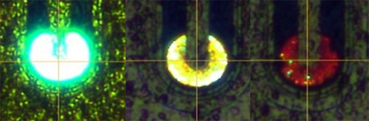
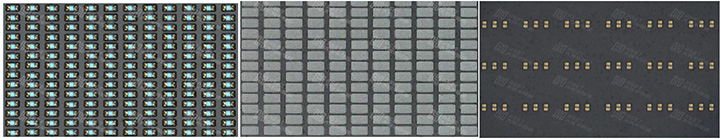
Fig. 2. (a) Each pixel under a scanning electron microscope (SEM). (b) The pixels after filling the quantum dots are placed under an ultraviolet fluorescence microscope [3].
TAG:
Guess you want to see it
Popular information
-
New progress in quantum dot patterning at Guangdong Academy of Sciences, suitable for Micro LEDs
-
Red MicroLED R &D competition accelerates: Material innovation can solve the problem of luminous eff

-
Or first for MicroLEDs! Fujian Institute of Paper Formosa develops efficient near-infrared quantum d
-
Micro LED Innovation Breakthrough: The future of display technology has arrived
-
Micro LED new breakthrough! Jingneng Optoelectronics's first 12-inch silicon substrate InGa-based tr
-
South Korean universities achieve growth of flexible GaN Micro LED arrays on graphene substrates
-
99.88% yield! Seoul National University Micro LED Mass Transfer New Breakthrough
-
Four Micro LED technologies achieve new progress
-
Domestic R &D team develops Micro LED high-efficiency backlight devices
-
BOE and Peking University announced new patents involving AR displays and Micro LED chips
the charts
- The best solution for AR glasses? Integrating Micro LEDs with advanced CMOS
- Red MicroLED R &D competition accelerates: Material innovation can solve the problem of luminous eff
- Micro LED heating capacity reduced by 40%! This study is supported by Samsung
- Zhejiang University's micro-level Micro-LED array achievements were selected into the top ten scient
- Red MicroLED R &D competition accelerates: Material innovation can solve the problem of luminous eff
- Analysis of huge transfer technology: How to break through the Micro LED display process problems?
- technology| Interpretation of MicroLED Technology in Mico Display Principles
- Micro LED achieves breakthrough results again
- Micro 0.4 released globally, opening a new era in the LED industry
- A team from Xiamen University designs artificial nanostructures that enhance deep ultraviolet light