Researchers from the two universities collaborated to develop laminated full-color Micro LEDs
- author:
- 2024-06-04 16:00:29
Recently, foreign media reported thatJapan's City University andSaudi Arabia's King Abdullah University of Science and Technology (KAUST) jointly developed a monolithic stacked RGB gallium nitride indium (GaInN) Micro LED array with a pixel density of 330PPI.
Researchers said that the product can be used in head-mounted smart devices such as AR/VR/MR. The micron-level pixel displays required by these devices cannot be manufactured through mechanical assembly technology, so monolithic manufacturing technology is needed.
Regarding the application of gallium nitride indium materials, the researchers explained that although gallium nitride indium based LEDs encounter major efficiency problems at longer wavelengths, gallium nitride indium has made new progress for red efficiency in the visible spectrum. In addition, compared with the commonly used red LED material aluminum gallium indium phosphide, the luminous efficiency of gallium indium LEDs is less affected by the reduction of the Micro LED's size.
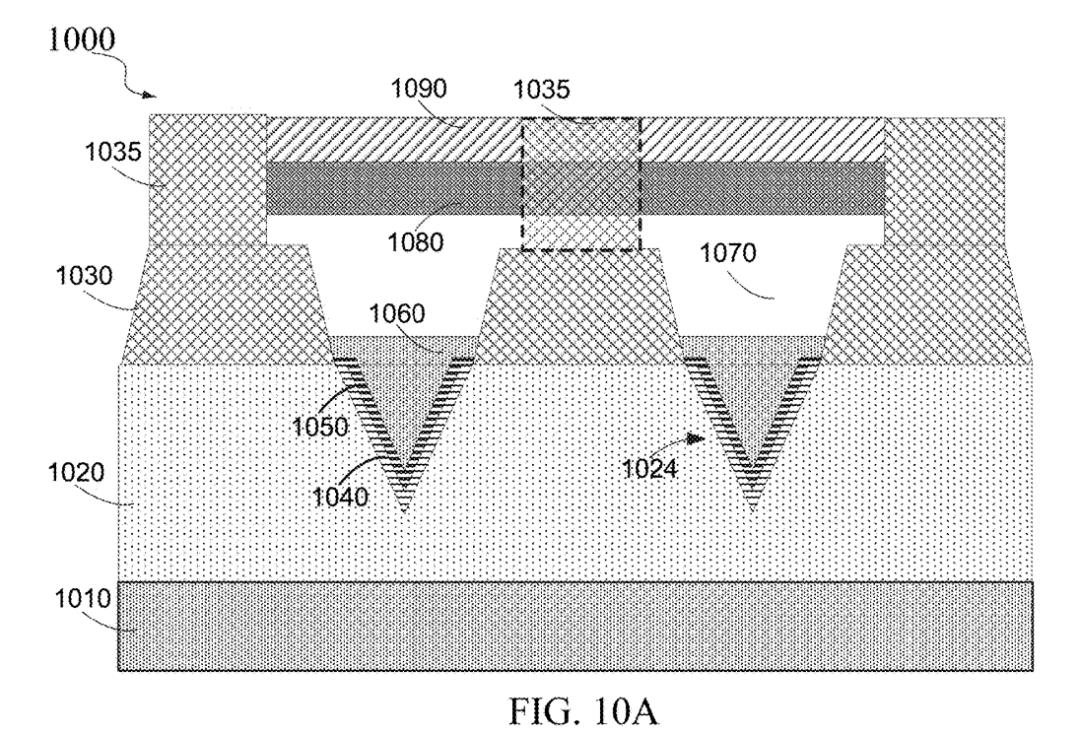
During the Micro LED epitaxial manufacturing stage, the research team used metal organic vapor phase epitaxy (MOVPE) technology to grow RGB Micro LED array materials on GaN substrates in two stages. Among them, the blue and green layers are grown by the Mingcheng University team, the KAUST team is responsible for the growth of the final red light stage, and the RGB layers are separated by Tunnel Junction (TJ).

Schematic cross-section of LED multi-stacked structure
In order to improve the luminous efficiency of the red layer, the red layer especially includes a superlattice epitaxial stack layer and red and blue single quantum wells (SQWs). Researchers said that inserting blue gallium nitride indium superlattice and gallium nitride indium SQW between the n-type GaN layer and the active layer in the red LED structure plays an effective role in improving the emission efficiency of red LEDs.
The researchers also pointed out that the GaN substrate used in Micro LEDs is very expensive, and for production, it is necessary to switch to cheaper materials, such as sapphire materials.
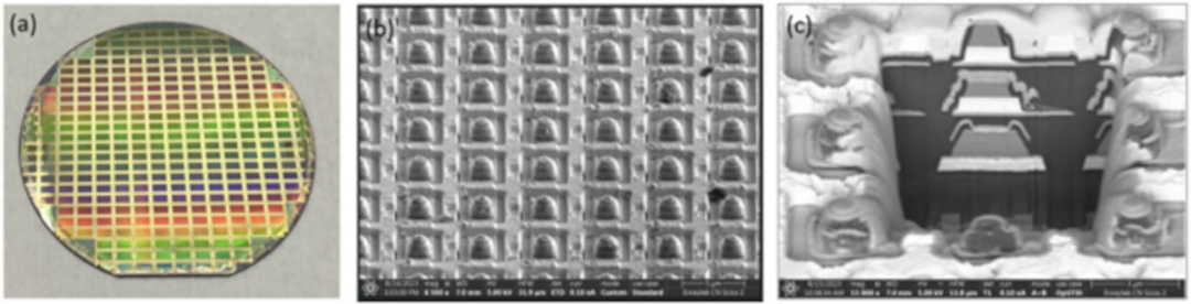
After epitaxial manufacturing is completed, the material is fabricated into RGB pixels with a density of 330PPI (see Figure 2). The Micro LED has a size of 73m x 20m, and the device mesa size is 35m x 15m.

Figure 2: Micro LED array process flow diagram
After testing by the researchers, data collected from the substrate side showed that the peak wavelengths of the electroluminescent (EL) spectrum of the blue-green-red Micro LED at a current density of 50A/cm ² were 486nm, 514nm and 604nm, respectively (Figure 3). The corresponding full width at half maximum (FWHM) are 29nm, 31nm and 52nm. The researchers said these values were similar to those for separately manufactured LED devices.

Electroluminescent (EL) Spectra of Blue-Green-Red Micro LED
At an injection current of 10A/cm ², the optical output power (LOP) of green Micro LEDs reaches almost 0.8W, and the LOP of red and blue light is less than 0.2W and 0.1W respectively.
TAG:
Guess you want to see it
Popular information
-
Meta patent disclosed that enables high quantum efficiency Micro LED pixels
-
Researchers from the two universities collaborated to develop laminated full-color Micro LEDs
-
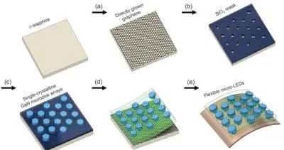
South Korean universities achieve growth of flexible GaN Micro LED arrays on graphene substrates
-
Red MicroLED R &D competition accelerates: Material innovation can solve the problem of luminous eff
-
The latest progress of Micro LED chips! 4 units disclosed
-
Micro 0.4 released globally, opening a new era in the LED industry
-
Huge transfer and breakthrough: 75,000 MicroLEDs can be transferred at a time
-
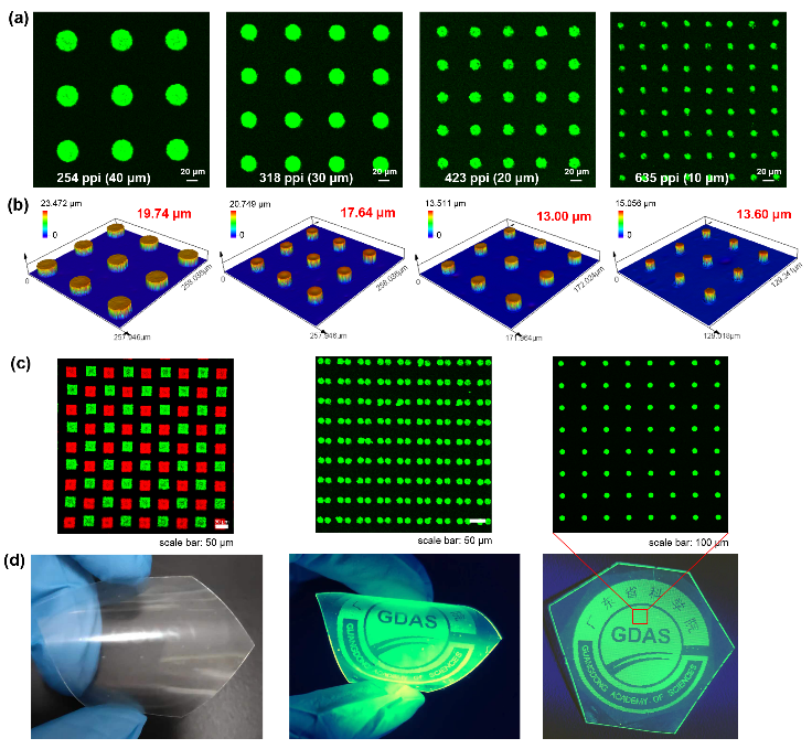
New progress in quantum dot patterning at Guangdong Academy of Sciences, suitable for Micro LEDs
-
Domestic R &D team develops Micro LED high-efficiency backlight devices
-
Analysis of the evolution path of Samsung Display XR Display's MicroLED microdisplay technology
the charts
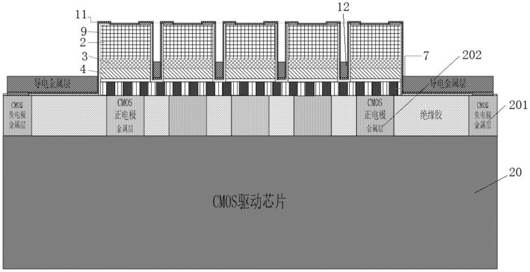
- The best solution for AR glasses? Integrating Micro LEDs with advanced CMOS
- Red MicroLED R &D competition accelerates: Material innovation can solve the problem of luminous eff
- Micro LED heating capacity reduced by 40%! This study is supported by Samsung
- Zhejiang University's micro-level Micro-LED array achievements were selected into the top ten scient
- Red MicroLED R &D competition accelerates: Material innovation can solve the problem of luminous eff
- Analysis of huge transfer technology: How to break through the Micro LED display process problems?
- technology| Interpretation of MicroLED Technology in Mico Display Principles
- Micro LED achieves breakthrough results again
- Micro 0.4 released globally, opening a new era in the LED industry
- A team from Xiamen University designs artificial nanostructures that enhance deep ultraviolet light