LED screen production technology: Micro-LED vs. Mini LED
- author:
- 2024-09-03 16:51:52
The initial task was to understand the application of Micro LEDs and Mini LEDs in the field of indoor LED screens. Because screens created using different technologies use terms such as micron, mini, and nano, this market is chaotic. Customers, in turn, repeat these infamous micro, mini and nano without thinking in the race for the coolest screen without realizing that these set-top boxes are nothing more than a marketing ploy.

进步就是进步,突飞猛进。Screens should be brighter, more saturated in colors, consume less, have less heat, etc. -scientists and engineers are working to improve powerful technical features-in every technical detail.
有进步的地方就有营销,营销人员使用各种营销工具来宣传营销人员不理解的东西。Market recognition and sales are important, but technology is secondary.
They are divided into internal screens and external screens. For permanent installation and leasing. All new technologies have resulted in improved technical characteristics of LED displays in terms of power supply, mounting base, new board, and spacing and size (i.e. pixels) of the LEDs themselves.
像素间距或节距是两个相邻 LED 中心之间的距离(以毫米为单位)。Every year, a micro-technological breakthrough occurs when one or another company introduces record-breaking smaller pixel spacing. By reducing the distance, the size of the LED itself is also reduced.
DIP -Direct series package. The technology is used on external screens, using separate LEDs for each color. Pixel spacing is greater than or equal to 6 mm.
SMD--表面贴装器件。This" three-in-one" technology is a traditional LED screen production technology. It is used for internal screens and external screens-LEDs, and three RGB LEDs have been installed at a certain spacing in its housing.
DIP 分色技术融入三种不同的外壳,可实现高色彩饱和度且易于安装。On the other hand, the SMD 3 in 1 has a more uniform overall color due to the use of RGB in one package. This is the standard technology used for high-quality LED screens. Surface mount technology is also used for external screens.
COB--板上芯片。The technology is used for internal screens by growing LEDs, which are also composed of three-color LEDs located directly on the board.

Almost all screens installed indoors use surface mount technology. To make an LED screen, each LED (also called a pixel) is required to be able to emit three colors: red, blue, and green-so each small LED contains a 3xLED, so the technology is called SMD 3in1.

简单且经过验证的技术。First, crystals are grown on a sapphire substrate, and then LEDs are manufactured. Subsequently, LED wall manufacturers purchased LEDs and used SMD technology to manufacture LED modules, and then assembled the video wall.
该工艺经过验证,易于安装和维护 - 即移除不工作的 LED,然后焊接一个新的 LED。There are subtle differences. Not all LEDs emit light in the same way, so when you buy a screen, you will buy the same batch of LEDs. There are also differences in the metals used in conductors-if it is gold, the quality will be higher, and in fact, the same is true for the cost of the LED itself and the finished screen. There is no difference when debugging, and the difference can only be seen after a while.
由于 LED 被焊接到电路板上,因此在对场所进行高质量清洁时,当用抹布擦拭屏幕时,小型 LED 会从其位置上脱落。After a while, the picture became less pleasing to the eye. However, these are all operational issues-after all, you can restrict the circle of people who have access to the screen.
当公司跨过 LED 之间距离小于 1 毫米的界限后,问 题就开始出现了。Because, in addition to the distance, the LEDs have also been reduced. First, the complexity of welding has increased, and secondly, the LEDs themselves have become difficult to fix in their position.
因此,我们想到了将每个SMD 3in1 LED组装成一组4个LED,然后将它们分组焊接的想法。
 IMD -Integrated installation equipment. IMD 4in1 surface mount technology represents not one SMD 3in1 LED, but a group of 4 such LEDs. Afterwards, due to the expansion of the platform, each group was welded to the main base. Currently, the market is mainly dominated by 4in1 groups, but 9in1 and 16in1 are expected to appear soon.
与此同时,像素间距变得更小,LED本身也变得更小,但安装的简便性仍然存在。Today, there are prototypes of screens manufactured using this technology with pitches of 0.5 mm and 0.6 mm. They were unveiled at ISE2020.
此外,为了保护这种像素间距的 LED,使用 GOB 和 AOB 技术来完全填充 LED,并且仅填充"腿"。
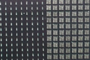 The left picture shows an example: on the left is an LED screen using COB technology, with no shell for each pixel, and on the right is using IMD4in1 technology.
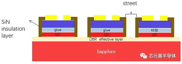
创建晶体和 LED 的另一种技术是直接在电路板上生长它们。This technology has long been known, but has only recently been widely used-for mounting LEDs on boards with very small pixel spacing.
该芯片还包含三个 RGB LED。According to this technology, the crystal can be inverted; no welding is needed because the crystal is grown on the plate. Therefore, future manufacturers plan to completely abandon soldering with small pixel pitches and eliminate the existing shortcomings of SMD technology.
 After growing LEDs, LED screen manufacturers using this technology will fill modules or cabinets with LEDs with special optically transparent compounds or gels to protect the LEDs.
屏幕变得光滑,类似于液晶面板的屏幕。One of the most immediate advantages is the ability to protect the LED strip from mechanical damage, such as during cleaning. It is clear that this compound does not provide protection against mechanical stress.
与传统的表面贴装SMD技术相比,COB可以在相同面积内实现更高的LED密度。As a result, higher pixelization uniformity is achieved for users.
技术发展的每个阶段都试图消除前一个阶段的缺点。For example, the design purpose of COB technology is to protect LEDs, especially very small LEDs, from damage, simplify the arrangement of ultra-small LEDs on the board, and further reduce heat dissipation and power consumption, but the most important thing is that it can be used Small pixels, no soldering problems.
与DIP和SMD技术相比,COB LED屏具有显着的优势。
Literally, it is a Micro LED. The expression used when the LED is less than one millimeter. When it comes to LED spheres, this is chip-on-board technology. It turns out to be a cool marketing strategy-sounds cool, micro LED.
现在我们来了解一下事实--谁以及什么叫 micro-LED。IMD 4in1 and COB technology are called Micro-LED by different manufacturing companies.
例如,我所了解的公司中,Leyard Planar在ISE 2020上展示了一款采用SMD 4in1技术的0.6mm间距的优秀屏幕。They call this technology microled.

自2012年起,索尼就开始推出基于COB技术的屏幕,称为CLEDIS--Crystal LED Integrated Structure,简称Crystal LED。The maximum screen spacing is 1.25 mm, the size is 19.2 x 5.4 meters, and the resolution is 16K (15360 x 4320), which is still in the leading position. Sony calls Crystal LED technology microLED.

三星连续几年推出了基于 COB 技术(倒装芯片 RGB LED)(也称为 microLED)的 0.84 毫米间距的高端 The Wall 屏幕。

在同一展会上,洲明展示了一款采用IMD4in1技术的0.5毫米间距的屏幕。Indeed, they are not called micro-ice; instead, the prefix nanometer appears.

康佳发布了一款采用microLED技术的LED灯条,最大对角线为236英寸。

与上述公司不同的是,中国制造商艾比森去年在 InfoComm China 2019 展会上,采用了 4in1 技术,将其称为 mini-LED(稍后我们会回到这项技术)。The pixel spacing is 0.9 mm. Subjectively, this is a strategically cool solution because it separates 4in1 and COB technology. But this is just marketing that has not yet taken root. Company representatives publicly stated that this was a publicity stunt.
Emissions or" self-emissions" are the only thing these technologies have in common. Similar! But their production technologies are completely different.

Micro LED 是一种用于创建 LED 画布的技术,这意味着构建视频墙时不受对角线限制,并且能够组装非标准屏幕形状。The leader has always been Sony, with a screen size of 63 x 17 feet, or 783 inches. Closely followed by Samsung, which launched the 292 today

进步就是进步,突飞猛进。Screens should be brighter, more saturated in colors, consume less, have less heat, etc. -scientists and engineers are working to improve powerful technical features-in every technical detail.
有进步的地方就有营销,营销人员使用各种营销工具来宣传营销人员不理解的东西。Market recognition and sales are important, but technology is secondary.
LED screen
They are divided into internal screens and external screens. For permanent installation and leasing. All new technologies have resulted in improved technical characteristics of LED displays in terms of power supply, mounting base, new board, and spacing and size (i.e. pixels) of the LEDs themselves.
像素间距或节距是两个相邻 LED 中心之间的距离(以毫米为单位)。Every year, a micro-technological breakthrough occurs when one or another company introduces record-breaking smaller pixel spacing. By reducing the distance, the size of the LED itself is also reduced.
LED production technology
DIP -Direct series package. The technology is used on external screens, using separate LEDs for each color. Pixel spacing is greater than or equal to 6 mm.
SMD--表面贴装器件。This" three-in-one" technology is a traditional LED screen production technology. It is used for internal screens and external screens-LEDs, and three RGB LEDs have been installed at a certain spacing in its housing.
DIP 分色技术融入三种不同的外壳,可实现高色彩饱和度且易于安装。On the other hand, the SMD 3 in 1 has a more uniform overall color due to the use of RGB in one package. This is the standard technology used for high-quality LED screens. Surface mount technology is also used for external screens.
COB--板上芯片。The technology is used for internal screens by growing LEDs, which are also composed of three-color LEDs located directly on the board.

Patch 3 in 1
Almost all screens installed indoors use surface mount technology. To make an LED screen, each LED (also called a pixel) is required to be able to emit three colors: red, blue, and green-so each small LED contains a 3xLED, so the technology is called SMD 3in1.

简单且经过验证的技术。First, crystals are grown on a sapphire substrate, and then LEDs are manufactured. Subsequently, LED wall manufacturers purchased LEDs and used SMD technology to manufacture LED modules, and then assembled the video wall.
该工艺经过验证,易于安装和维护 - 即移除不工作的 LED,然后焊接一个新的 LED。There are subtle differences. Not all LEDs emit light in the same way, so when you buy a screen, you will buy the same batch of LEDs. There are also differences in the metals used in conductors-if it is gold, the quality will be higher, and in fact, the same is true for the cost of the LED itself and the finished screen. There is no difference when debugging, and the difference can only be seen after a while.
由于 LED 被焊接到电路板上,因此在对场所进行高质量清洁时,当用抹布擦拭屏幕时,小型 LED 会从其位置上脱落。After a while, the picture became less pleasing to the eye. However, these are all operational issues-after all, you can restrict the circle of people who have access to the screen.
当公司跨过 LED 之间距离小于 1 毫米的界限后,问 题就开始出现了。Because, in addition to the distance, the LEDs have also been reduced. First, the complexity of welding has increased, and secondly, the LEDs themselves have become difficult to fix in their position.
因此,我们想到了将每个SMD 3in1 LED组装成一组4个LED,然后将它们分组焊接的想法。
IMD 4 in 1
 IMD -Integrated installation equipment. IMD 4in1 surface mount technology represents not one SMD 3in1 LED, but a group of 4 such LEDs. Afterwards, due to the expansion of the platform, each group was welded to the main base. Currently, the market is mainly dominated by 4in1 groups, but 9in1 and 16in1 are expected to appear soon.
 与此同时,像素间距变得更小,LED本身也变得更小,但安装的简便性仍然存在。Today, there are prototypes of screens manufactured using this technology with pitches of 0.5 mm and 0.6 mm. They were unveiled at ISE2020.
此外,为了保护这种像素间距的 LED,使用 GOB 和 AOB 技术来完全填充 LED,并且仅填充"腿"。
COB--chip on board
 The left picture shows an example: on the left is an LED screen using COB technology, with no shell for each pixel, and on the right is using IMD4in1 technology.
 创建晶体和 LED 的另一种技术是直接在电路板上生长它们。This technology has long been known, but has only recently been widely used-for mounting LEDs on boards with very small pixel spacing.
该芯片还包含三个 RGB LED。According to this technology, the crystal can be inverted; no welding is needed because the crystal is grown on the plate. Therefore, future manufacturers plan to completely abandon soldering with small pixel pitches and eliminate the existing shortcomings of SMD technology.
 After growing LEDs, LED screen manufacturers using this technology will fill modules or cabinets with LEDs with special optically transparent compounds or gels to protect the LEDs.
 屏幕变得光滑,类似于液晶面板的屏幕。One of the most immediate advantages is the ability to protect the LED strip from mechanical damage, such as during cleaning. It is clear that this compound does not provide protection against mechanical stress.
与传统的表面贴装SMD技术相比,COB可以在相同面积内实现更高的LED密度。As a result, higher pixelization uniformity is achieved for users.
技术发展的每个阶段都试图消除前一个阶段的缺点。For example, the design purpose of COB technology is to protect LEDs, especially very small LEDs, from damage, simplify the arrangement of ultra-small LEDs on the board, and further reduce heat dissipation and power consumption, but the most important thing is that it can be used Small pixels, no soldering problems.
与DIP和SMD技术相比,COB LED屏具有显着的优势。
- The depth is smaller. By allowing the use of thinner plates, manufacturers can reduce the thickness of the overall structure. As a result, the overall weight of the screen will be reduced. The increase in structural thickness, the ability not to reinforce certain types of walls, and the ultimate cost.
- Increased viewing angle. The screen based on SMD technology is created by installing three LEDs inside the housing, thereby placing the RGB LEDs in a small groove. In addition, factors such as replacing LEDs, reinstalling LEDs, and uneven masks can also increase the difficulty. As a result, the viewing angle decreases and becomes uneven.
SMD--120 - 140 degrees;
COB exceeds 170 degrees.
COB – 超过 170 度。
*尽管在实践中,使用COB的制造商并不声称超过160度。
另一方面,SMD技术也实现了更大的可视角度。 - The possibility of bending. The curved shape of the PCB will not damage the COB LED chip, and when using SMD technology to bend the PCB, the bending angle has great limitations.
- Better thermal performance, lower power consumption at the same brightness level, higher contrast and shortest response time.
- By filling the housing with a special compound, the protection of the LED itself is increased, which affects the service life of the LED. However, on the other hand, there is no possibility of maintainability for the foreseeable future.
Micro-LED& COB
Literally, it is a Micro LED. The expression used when the LED is less than one millimeter. When it comes to LED spheres, this is chip-on-board technology. It turns out to be a cool marketing strategy-sounds cool, micro LED.
现在我们来了解一下事实--谁以及什么叫 micro-LED。IMD 4in1 and COB technology are called Micro-LED by different manufacturing companies.
例如,我所了解的公司中,Leyard Planar在ISE 2020上展示了一款采用SMD 4in1技术的0.6mm间距的优秀屏幕。They call this technology microled.

自2012年起,索尼就开始推出基于COB技术的屏幕,称为CLEDIS--Crystal LED Integrated Structure,简称Crystal LED。The maximum screen spacing is 1.25 mm, the size is 19.2 x 5.4 meters, and the resolution is 16K (15360 x 4320), which is still in the leading position. Sony calls Crystal LED technology microLED.

三星连续几年推出了基于 COB 技术(倒装芯片 RGB LED)(也称为 microLED)的 0.84 毫米间距的高端 The Wall 屏幕。

在同一展会上,洲明展示了一款采用IMD4in1技术的0.5毫米间距的屏幕。Indeed, they are not called micro-ice; instead, the prefix nanometer appears.

康佳发布了一款采用microLED技术的LED灯条,最大对角线为236英寸。

与上述公司不同的是,中国制造商艾比森去年在 InfoComm China 2019 展会上,采用了 4in1 技术,将其称为 mini-LED(稍后我们会回到这项技术)。The pixel spacing is 0.9 mm. Subjectively, this is a strategically cool solution because it separates 4in1 and COB technology. But this is just marketing that has not yet taken root. Company representatives publicly stated that this was a publicity stunt.
Micro LEDs and OLEDs
Emissions or" self-emissions" are the only thing these technologies have in common. Similar! But their production technologies are completely different.

Micro LED 是一种用于创建 LED 画布的技术,这意味着构建视频墙时不受对角线限制,并且能够组装非标准屏幕形状。The leader has always been Sony, with a screen size of 63 x 17 feet, or 783 inches. Closely followed by Samsung, which launched the 292 today
TAG:
Guess you want to see it

Popular information
-
The total investment exceeds 26 billion yuan! This year's Mini/Micro LED is something to watch!
-
Analysis of Mini/Micro LED driving technology
-
The latest research on UV LED solves 2 problems
-
Division 5184! TCL launches Mini LED TV with peak brightness of 5000nit
-
LED screen production technology: Micro-LED vs. Mini LED
-
MIT researchers demonstrate perovskite nanoscale LED arrays
-
Milestone breakthrough? UVC-LED new lens appears
-
This company has obtained invention patents related to MINI LED
-
The internal quantum efficiency has been increased to 70%, and this team has made a breakthrough in
-
JCDecaux Chemical Corporation: The development of new Mini display-related products is progressing,
the charts
- JCDecaux Chemical Corporation: The development of new Mini display-related products is progressing,
- The total investment exceeds 26 billion yuan! This year's Mini/Micro LED is something to watch!
- Involving key patents involving Mini LED, Zhaoyuan Optoelectronics, Xinruida, etc. disclosed...
- Division 5184! TCL launches Mini LED TV with peak brightness of 5000nit
- Mini/Micro LED equipment manufacturer Keyun Laser has completed Series B financing of over RMB 100 m
- Lenovo releases a new 34-inch hairtail display equipped with Mini LED backlight technology
- POB and COB: Who will dominate the future of Mini LED applications?
- The internal quantum efficiency has been increased to 70%, and this team has made a breakthrough in
- High-precision optical processing, this team used MINI-LED technology as a breakthrough point
- Analysis of Mini/Micro LED driving technology