High-precision optical processing, this team used MINI-LED technology as a breakthrough point
- author:
- 2024-06-04 15:05:41
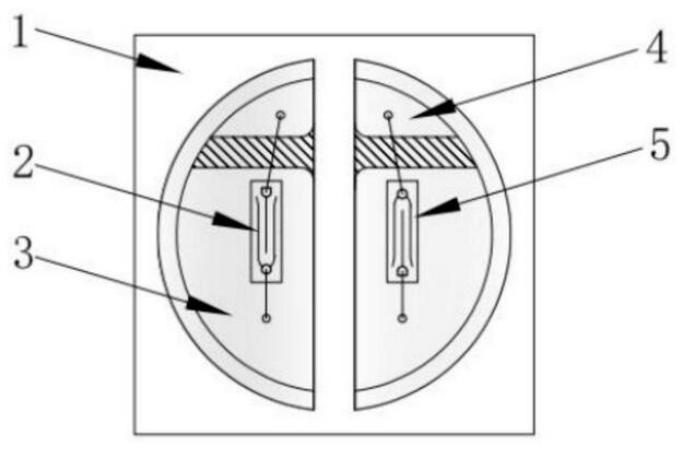
In order to achieve low-cost and high-precision optical processing, the research team of Dr. Zheng Lei from the University of Hanover in Germany proposed a projection lithography method that uses MINI-LED as the light source and transfers the pattern to the substrate through standard optical elements and microscope objectives. -MINI-LED microscope projection lithography (MPP), and based on this, a simple, low-cost, easy-to-operate MPP device (as shown in Figure 1a) has been developed to achieve fast and high-resolution 2D micro-nano optical device processing.

Figure 1: MPP device schematic diagram (a) and complete processing process diagram (b)
In order to make it easier to prepare the templates needed for processing, the researchers have also developed a complete set of processes covering structural design and printing, chromium mask preparation to MPP processing of optical devices (the schematic diagram is shown in Figure 1b). When preparing the chromium mask, the researchers compared the accuracy and quality of transferring the structural pattern on the transparent sheet to the blank chromium mask using ordinary aspheric lenses and Tessar lenses respectively, and optimized the optical system of this process. Using the prepared mask, researchers can use MPP to process the final optical structure.
In order to explore the high-precision processing performance of this method, the researchers also processed single-wire structures with different feature size and achieved a feature size below 100 nanometers.

Figure 3: Grating structure of microscope objective lenses processed by different manufacturers and different NA values
At the same time, the researchers also used objective lenses of different price points/manufacturers and different NA values to process the grating structure to verify the stability and reliability of the method in high-precision micro-nano processing.
TAG:
Guess you want to see it

Popular information
-
Involving key patents involving Mini LED, Zhaoyuan Optoelectronics, Xinruida, etc. disclosed...
-
MIT researchers demonstrate perovskite nanoscale LED arrays
-
POB and COB: Who will dominate the future of Mini LED applications?
-
This company has obtained invention patents related to MINI LED
-
Milestone breakthrough? UVC-LED new lens appears
-
The latest research on UV LED solves 2 problems
-
The internal quantum efficiency has been increased to 70%, and this team has made a breakthrough in
-
Australia company Silanna UV achieves mass production of ultraviolet LEDs
-
Division 5184! TCL launches Mini LED TV with peak brightness of 5000nit
-
LED screen production technology: Micro-LED vs. Mini LED
the charts
- JCDecaux Chemical Corporation: The development of new Mini display-related products is progressing,
- The total investment exceeds 26 billion yuan! This year's Mini/Micro LED is something to watch!
- Involving key patents involving Mini LED, Zhaoyuan Optoelectronics, Xinruida, etc. disclosed...
- Division 5184! TCL launches Mini LED TV with peak brightness of 5000nit
- Mini/Micro LED equipment manufacturer Keyun Laser has completed Series B financing of over RMB 100 m
- Lenovo releases a new 34-inch hairtail display equipped with Mini LED backlight technology
- POB and COB: Who will dominate the future of Mini LED applications?
- The internal quantum efficiency has been increased to 70%, and this team has made a breakthrough in
- High-precision optical processing, this team used MINI-LED technology as a breakthrough point
- Analysis of Mini/Micro LED driving technology