Australia company Silanna UV achieves mass production of ultraviolet LEDs
- author:
- 2024-06-04 15:26:04
Recently, Australia company Silanna UV used Veeco GEN200MBE tool to produce 150 mm GaN epitaxial wafers on sapphire substrates and manufactured more than 10000 functional devices. After packaging, these ultraviolet LEDs can produce an output power of 1.7mW at peak efficiency, and have a service life of thousands of hours.
Jordan Nichols, senior device integration engineer at Silanna, said: The Veeco GEN200 platform is a dual-chamber system, so we have the ability to meet current needs. quot; He revealed that the company's outreach facilities were specifically built to expand production capacity as demand grows.

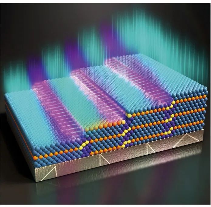
To form the epitaxial structure of the LED, Silanna's engineers first deposited a 400-nm-thick aluminum nitride buffer layer, then four different superlattices, and finally a p-type gallium nitride layer (see photo). The superlattice used for the recombination region is about 80 nm thick, has 36 periods, and the layer width can be adjusted according to the target wavelength, which can range from 229 nm to 240 nm.
An advantage of using short-period superlattices as active regions at the same time is that their strip structure can promote lateral electrical emission, thereby improving light extraction efficiency. Compared to traditional quantum well regions used for extreme ultraviolet LEDs, this form of active region also reduces dopant ionization energy, thereby reducing resistivity. Silanna uses standard lithography and metallization processes to produce LEDs from its epitaxial wafers. After forming the grid by dry etching, titanium/aluminum contacts are deposited to form electrical contacts. After adding a standard passivation layer, the company's engineers can use an integrating sphere to perform optoelectronic measurements at the wafer level.
Wafer-level maps of electroluminescence spectra of more than 10000 LEDs driven with a current of 20 mA were recorded. The emission wavelength of these devices is approximately 233 nm, the standard deviation of the peak wavelength of the device 100 mm in the middle of the wafer is only 0.16 nm, and the average optical power is 0.2 W.
Silanna produced packaged LEDs by cutting 1 mm by 1 mm devices on the epitaxial wafer into small pieces, thinning the substrate to 275 mm and polishing it, and then flip-chip the die onto an aluminum nitride ceramic package. These devices have a peak wall insertion efficiency of 0.55% at 50 mA. When the current is increased to 1A, the output power climbs to 17.4 mW, which is said to be the highest radiant flux of a far-ultraviolet LED grown on sapphire.
Lifetime testing of 80 packaged devices driven at 20 mA showed a lifetime of 2800 hours, which is based on the time required for the radiant flux to reduce to 70% of its original value.
Silanna UV said that although MOCVD is the most commonly used growth method for the production of extreme ultraviolet LEDs, MBE can also produce these devices in large quantities and with high yields.
TAG:
Guess you want to see it

Popular information
-
Involving key patents involving Mini LED, Zhaoyuan Optoelectronics, Xinruida, etc. disclosed...
-
The latest research on UV LED solves 2 problems
-
The internal quantum efficiency has been increased to 70%, and this team has made a breakthrough in
-
LED screen production technology: Micro-LED vs. Mini LED
-
Milestone breakthrough? UVC-LED new lens appears
-
POB and COB: Who will dominate the future of Mini LED applications?
-
High-precision optical processing, this team used MINI-LED technology as a breakthrough point
-
Korea Photonics Technology Research Institute says the efficiency of Micro LED technology has been g
-
This company has obtained invention patents related to MINI LED
-
Australia company Silanna UV achieves mass production of ultraviolet LEDs
the charts
- JCDecaux Chemical Corporation: The development of new Mini display-related products is progressing,
- The total investment exceeds 26 billion yuan! This year's Mini/Micro LED is something to watch!
- Involving key patents involving Mini LED, Zhaoyuan Optoelectronics, Xinruida, etc. disclosed...
- Division 5184! TCL launches Mini LED TV with peak brightness of 5000nit
- Mini/Micro LED equipment manufacturer Keyun Laser has completed Series B financing of over RMB 100 m
- Lenovo releases a new 34-inch hairtail display equipped with Mini LED backlight technology
- POB and COB: Who will dominate the future of Mini LED applications?
- The internal quantum efficiency has been increased to 70%, and this team has made a breakthrough in
- High-precision optical processing, this team used MINI-LED technology as a breakthrough point
- Analysis of Mini/Micro LED driving technology