What is the difference between GOB and COB displays?
- author:
- 2024-05-27 16:43:21
In the development of technology, mistakes and trial and error are inevitable. However, GOB cannot be called a real technology, because a team trying to replicate COB technology wanted to find a commercial shortcut after encountering difficulties.
1. The origin of GOB
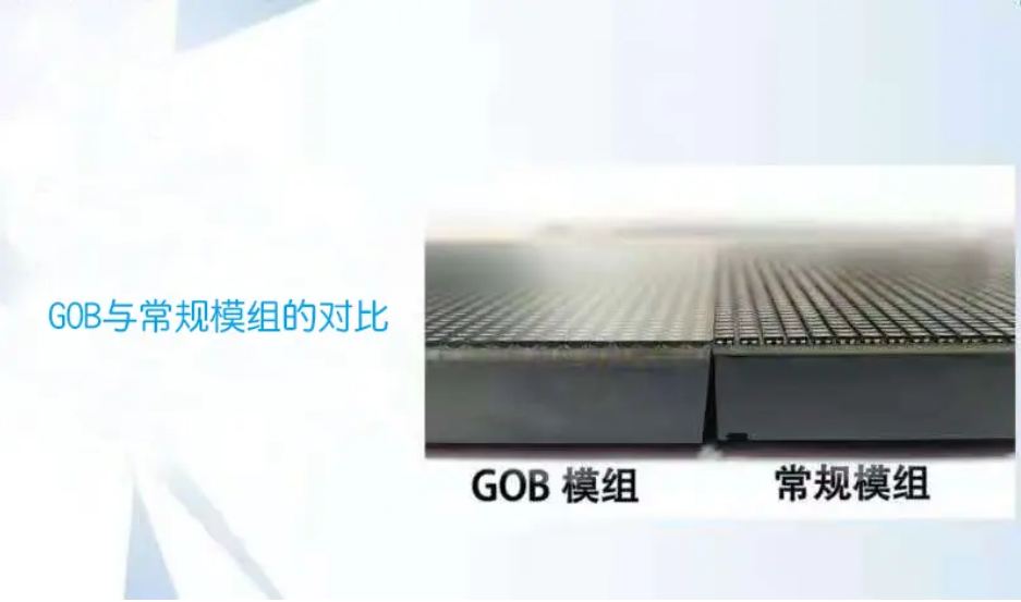
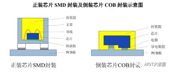
As we all know, the three major packaging technologies of DIP, SMD, and COB all involve LED chip-level technologies. GOB does not protect LED chips. It just applies glue to the bracket PIN pins of SMD devices on the SMD module. A protective process for injection protection.
众所周知,DIP、SMD、COB 这三大封装技术都是涉及到 LED 芯片级别的技术,而 GOB 并没有对 LED 芯片进行保护,它只是在 SMD 的模组上,对 SMD 器件的支架 PIN 脚进行灌胶保护的一种防护工艺。Therefore, if you insist on calling it a technology, it can only be regarded as a module-level protection technology.
3. Positioning of GOB process
DIP 和 SMD 技术都是 1.0 版的 LED 显示面板集成技术的代表技术。
COB 集成封装技术是 2.0 版的 LED 显示面板集成技术的代表技术。
四、结论
1. The origin of GOB
- Timing for launch: GOB was launched after eight years of research and development of COB technology and its development direction had been recognized by the industry.
- GOB Group: COB's English is Chip On Borad, which translates literally as chip on the board; while GOB's English is Glue On Board, which translates literally as glue on the board.
As we all know, the three major packaging technologies of DIP, SMD, and COB all involve LED chip-level technologies. GOB does not protect LED chips. It just applies glue to the bracket PIN pins of SMD devices on the SMD module. A protective process for injection protection.
众所周知,DIP、SMD、COB 这三大封装技术都是涉及到 LED 芯片级别的技术,而 GOB 并没有对 LED 芯片进行保护,它只是在 SMD 的模组上,对 SMD 器件的支架 PIN 脚进行灌胶保护的一种防护工艺。Therefore, if you insist on calling it a technology, it can only be regarded as a module-level protection technology.
3. Positioning of GOB process
- Integrated technical characteristics of version 1.0 of LED display panels
- Single lamp bead discretely packaged lamp bead device
- Supported packaging technology
- Post-packaged display panel integration technology
- Industrial chain form: upstream (LED chips)+ midstream (packaging)+ downstream (display factory)
DIP 和 SMD 技术都是 1.0 版的 LED 显示面板集成技术的代表技术。
- Integrated technical characteristics of version 2.0 of LED display panels
- Multi-lamp bead integrated on-board packaging lamp bead device
- stentless packaging technology
- Display panel integration technology in package
- Industrial chain form: upstream (LED chips)+ downstream (packaging panel factory)
COB 集成封装技术是 2.0 版的 LED 显示面板集成技术的代表技术。
- GOB process positioning
- Has all the features of version 1.0 of LED display panel integration technology:
- Single lamp bead discretely packaged lamp bead device
- Supported packaging technology
- Post-packaged display panel integration technology
- Industrial chain form: upstream (LED chips)+ midstream (packaging)+ downstream (display factory)
- The GOB process is just a glue protection treatment process for the surface of display panels downstream of the traditional industrial chain (display factory). It is a process that can only be carried out after the SMT process is completed.
- Has all the features of version 1.0 of LED display panel integration technology:
四、结论
- GOB is not an LED chip-level packaging technology. It is just a panel protection treatment process after the SMT process of version 1.0 of the LED display panel integration technology in industrial downstream display factories.
- The GOB display panel is an SMD display panel, and it still cannot solve all the problems of bracket technology.
- Although GOB display panels can improve the hardware protection capabilities and appearance consistency of surface lamp beads, the resulting internal stress release problems, heat dissipation problems, repair problems, and poor colloid affinity problems will deteriorate the working performance of the display panels.
- In outdoor and rental transparent display applications, GOB display panels do not have reliable outdoor protection and collision resistance.
- To sum up, the GOB concept is a business activity.
TAG:
Guess you want to see it

Popular information
-
Analysis of COB mid-to-high-end PCB design process through 3D pictures
-
Three main development directions of COB packaging technology
-
What are the LED chip packaging materials used to package COBs?
-
Expand another 1100 COB production lines, and the MLED display card displays the "Big Era"
-
Exploring the secret of LED screen production: Process comparison between COB technology and SMD tec
-
An article clearly understands what GOB is in led display protection technology, what are the advant
-
Detailed explanation of COB packaging process: the key to improving product quality

-
COB flushing, rear packaging attracts attention
-
LED dynamic multiplexing pixel technology for COB and COG panels
-
Analyze outdoor COB display screens from Asian Games events
the charts
- Technical analysis of COB, IMD, mini, micro LED market
- Expand another 1100 COB production lines, and the MLED display card displays the "Big Era"
- COB flushing, rear packaging attracts attention
- What is the difference between GOM,COB, and msd packages?
- Which of the two technologies is the mainstream route, MIP or COB?
- LED dynamic multiplexing pixel technology for COB and COG panels
- Detailed explanation of COB packaging process: the key to improving product quality
- Analyze outdoor COB display screens from Asian Games events
- Exploring the secret of LED screen production: Process comparison between COB technology and SMD tec
- What are the LED chip packaging materials used to package COBs?