Exploring the secret of LED screen production: Process comparison between COB technology and SMD tec
- author:
- 2024-05-27 11:19:16
As an important representative of modern display technology, LED screens have continued to evolve their production process. COB technology and SMD technology are two commonly used processes in the production of LED screens. This article will explore in depth the differences between these two technologies and help readers better understand the mystery of the LED screen production process.
1. Process introduction
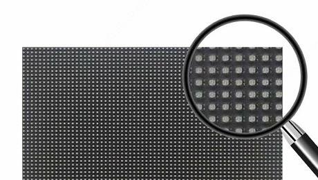
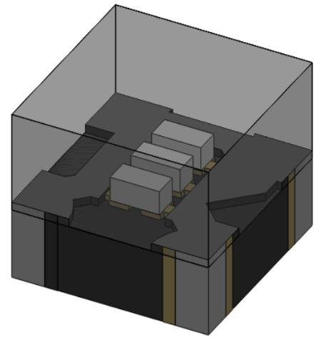
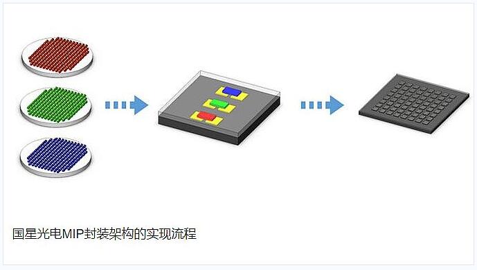
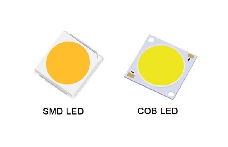
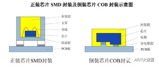
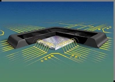
The SMD technology route is to package the light-emitting chips (wafers) into lamp beads, solder the lamp beads to the PCB board to form a unit module, and finally splice them into a whole LED screen;
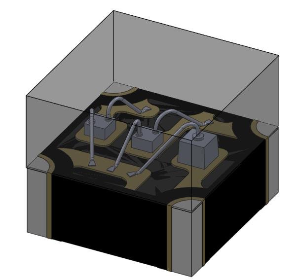
The COB technical route is to directly solder the optical chip (wafer) on the PCB board, then coat the entire film to form a unit module, and finally splice it into a whole LED screen.
2. Product differences
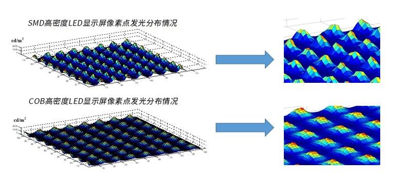
01
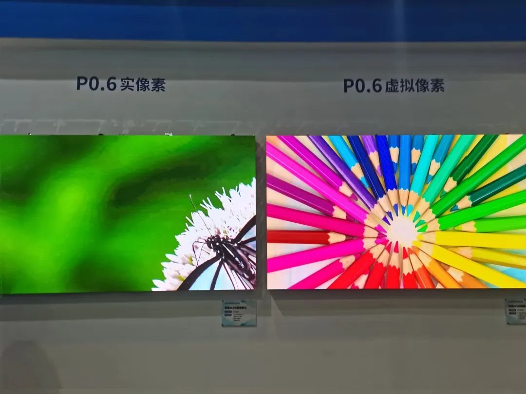
|图像差异
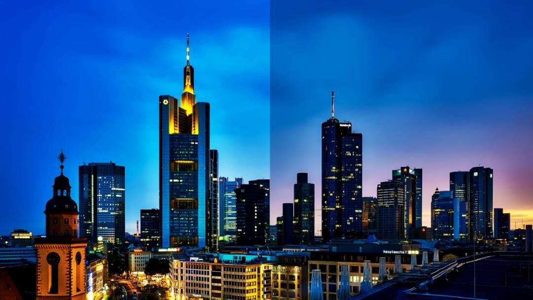
The SMD screen lamp beads emit light as single members, showing a point light source effect. Because the COB screen is covered with the entire light emitting chip, the light source becomes a surface light source after being scattered and refracted by the coating. Compared with point light sources, surface light sources have a better overall visual appearance, have no graininess when viewing, and can reduce the stimulation of the light source to the human eye, making them more suitable for long-term close-up viewing.
After the COB screen is completely packaged with a new process, the contrast ratio can be higher, reaching more than 20000:1. The contrast ratio of the SMD screen will not exceed 10000:1. In contrast, the viewing effect of the COB screen when viewed on the front is closer to the LCD screen, with bright colors and better details.
However, since COB screens cannot sort individual lamp beads with similar optical properties like SMD screens, the entire screen needs to be corrected before leaving the factory. Although the front viewing effect is excellent, color inconsistency is prone to occur when side viewing at large angles.
02
|可靠性差异
LED screens with SMD technology, because the light-emitting chips are packaged first and then mounted, have weak overall protection and are easy to knock off the lights. They have poor waterproof, moisture-proof and dustproof properties and cannot be wiped. However, on-site maintenance is convenient and conducive to later maintenance.
The LED screen of COB technology uses a chip to be directly pasted and then covered with the whole film. The overall protection is good. The front protection level can reach IP65. It can be effectively waterproof, moisture-proof, and anti-bump. It can be cleaned with a wet towel. However, due to the overall film, it cannot be repaired on site and needs to be returned to the factory for repair with professional equipment, which is inconvenient.

03
|能效差异
Most of the luminescent chips in the lamp beads of the mainstream SMD screen products are form-fitting technology, with leads blocking the light source. While COB screens are mostly flip-chip technology, with no blocking of the light source. Therefore, when the same brightness is achieved, the COB screen consumes lower power and has a better economy to use.
Dress inverted
In addition, due to the low transparency of the epoxy resin used in SMD lamp bead packaging, the overall coating film used in COB screens has high transparency, further improving the cost-effective use of COB screens.
04
|成本差异
SMD's production process and process are relatively complex, but due to the low technical threshold, there are more than a thousand manufacturers across the country, with sufficient competition and relatively mature technological development.
COB's production process has a high technical threshold, and only less than 20 manufacturers across the country have R & D, production and manufacturing capabilities.
COB technology is still developing rapidly. Although its theoretical cost is lower than that of SMD screens, due to the low product yield, the current cost of COB screens still has a certain disadvantage compared to SMD screens with a spacing above 1.2.
By comparing COB technology and SMD technology, we can see that they each have their own advantages and characteristics. In practical applications, the selection of the appropriate production process should be determined based on specific needs and application scenarios. With the continuous development of technology, we can expect that the LED screen production process will continue to innovate and improve, bringing us better display effects and experiences. I hope this article can provide readers with useful reference and let us look forward to a bright future for LED screen technology.
TAG:
Guess you want to see it


Popular information
-
COB technology helps display enter the era of p0.XXmm HD
-
Which of the two technologies is the mainstream route, MIP or COB?
-
How to view the reasons for poor consistency of COB ink?

-
COB flushing, rear packaging attracts attention
-
What is the difference between GOM,COB, and msd packages?
-
The difference between COB package and traditional SMD package
-
LED dynamic multiplexing pixel technology for COB and COG panels
-
What are the LED chip packaging materials used to package COBs?
-
Common comparisons between LED displays COB and GOB: Detailed explanation of advantages and disadvan
-
Three main development directions of COB packaging technology
the charts
- Technical analysis of COB, IMD, mini, micro LED market
- Expand another 1100 COB production lines, and the MLED display card displays the "Big Era"
- COB flushing, rear packaging attracts attention
- What is the difference between GOM,COB, and msd packages?
- Which of the two technologies is the mainstream route, MIP or COB?
- LED dynamic multiplexing pixel technology for COB and COG panels
- Detailed explanation of COB packaging process: the key to improving product quality
- Analyze outdoor COB display screens from Asian Games events
- Exploring the secret of LED screen production: Process comparison between COB technology and SMD tec
- What are the LED chip packaging materials used to package COBs?