The difference between COB package and traditional SMD package
- author:
- 2024-05-27 11:37:43
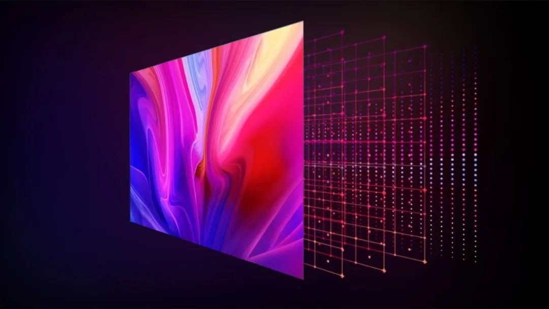
In the field of LED display applications, COB packaging has gradually matured, especially in the field of outdoor small spacing with its unique technical advantages. In the past two years, with the improvement of production technology and process, COB packaging technology has made qualitative breakthroughs, and the factors that once restricted its development have also been resolved one by one in technological innovation. So, what are the technical advantages of COB packaging? What are the differences between it and traditional SMD packages? Will it replace SMD and become the mainstream of LED displays in the future?
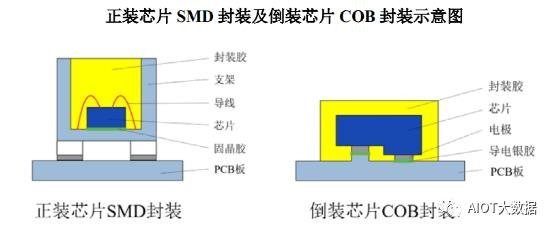
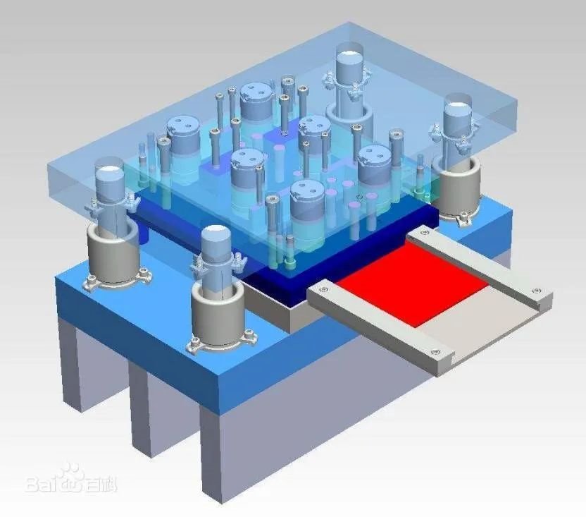
COB packaging is to directly fix the LED chip on the solder pad of the lamp bead position of the PCB board using conductive glue and insulating glue, and then solder the conduction performance of the LED chip. After testing well, it is encapsulated with epoxy resin glue.
COB 封装是将 LED 芯片直接利用导电胶和绝缘胶固定在 PCB 板灯珠灯位的焊盘上,随后进行 LED 芯片导通性能的焊接,测试良好后用环氧树脂胶包封。
SMD packaging uses conductive glue and insulating glue to fix the LED chip on the solder pad of the lamp bead bracket, and then uses the same conduction performance as the COB package to solder. After performance testing, it is encapsulated with epoxy resin glue, and then carries out Light dividing, cutting and taping operations, and then transported to the screen factory.
02 Comparison of advantages and disadvantages
There is no doubt that SMD packaging factories have the ability to manufacture high-quality lamp beads, but the production processes are numerous and the costs are relatively high, and the transportation, material storage and quality control costs from the lamp bead packaging factory to the screen factory will also increase.
SMD believes that COB packaging technology is too complex, and the one-pass rate of the product is difficult to control. It even regards it as an insurmountable obstacle, with problems such as inability to repair failure points and low yield.
In fact, with the current level of equipment technology and quality control, the 0.5K integrated technology of COB packaging can achieve a one-time pass rate of about 70%, the 1K integrated technology can reach about 50%, and the 2K integrated technology can allow this indicator to reach about 30%. Even if there are modules that fail to pass the pass rate test once, there are usually only 1-5 defective points on the entire board, and there are very few modules with more than 5 defective points. After testing and repairing before sealing, the qualified rate of finished products can be achieved. Up to about 90%-95%. And with technological progress and experience accumulation, this indicator will continue to improve. At the same time, we also have point-by-point repair technology for defective dots after sealing.
03 Technical analysis and evaluation
Difficulty of technical implementation:
SMD packaging: Obviously, this single-lamp bead singulation packaging technology has accumulated many years of practical experience. Each family has unique skills and scale. The technology is mature and it is relatively easy to implement.
COB packaging: As a new packaging technology integrated with multiple lamp beads, technical experience in production equipment, production process equipment, testing and testing methods and many other aspects in practice needs to be continuously accumulated and verified in innovative practice. The technical threshold is high and difficult, and the biggest challenge currently facing is how to improve the one-time pass rate of the product. COB packaging is facing a technological peak. Although it is not insurmountable, it is relatively difficult to implement.
Factory failure rate control level:
Both COB and SMD packages can control the failure rate very well, and ensure zero failure rate when delivered to customers.
Cost control:
In theory, COB should have a slight advantage in cost control in this aspect, but the current production capacity is limited and scale has not yet been formed, so SMD still has the advantage for the time being.
Reliability hazards:
The four-corner or hexagonal brackets used in SMD packages bring technical difficulties and reliability hazards to subsequent production. For example, the lamp bead surface over-reflow soldering process needs to solve the problem of welding yield of a large number of bracket pins. If SMD is used outdoors, the problem of outdoor protection yield of bracket pins needs to be solved.
However, COB technology eliminates the need for brackets, and there are almost no major technical difficulties and reliability hazards in subsequent production processes. It only faces two technical problems: one is how to ensure that the IC driver chip surface does not appear when the IC driver chip surface is reflowed. Failure points are not present on the surface, and the other is how to solve the problem of module ink consistency.
The friendliness of the application process:
The COB packaging lamp beads are fixed on the PCB board by epoxy resin. The affinity between the epoxy resin adhesive and the PCB board is extremely strong. They have the following physical properties: compressive strength is 8.4kg/mm2, shear strength is 4.2kg/mm2, impact strength is 6.8kg*cm/cm2, and hardness is Shore D 84. Therefore, it is not afraid of static electricity, bumps, and impacts, can be bent and deformed, is wear-resistant, easy to clean, has strong contact with people and the environment, is not squeamish and durable.
The SMD package lamp beads are soldered on the PCB board through bracket pins. The physical strength test performance is not high. They are delicate and afraid of touching, afraid of electrostatic failure caused by touch, and are not very contact-friendly with people and the environment.
04 Competition issues:
Since COB packaging has not yet formed large-scale production capacity, it currently has not formed a cost advantage at the P8-P10 level. It only has application advantages in outdoor displays that need not be afraid of collisions such as sports venues and rental markets, as well as special application environments such as high and low temperatures, humidity, and salt fog. At the P5-P6 level, the cost is already comparable to SMD. In pure outdoor applications at P4-P3 and even denser levels, the cost will occupy an absolute advantage. Once production capacity is formed in the future, COB packaging will have price advantages at all point density levels, and there is currently no competition among COB peers.
SMD faces competition among peers. As mentioned above, the quality of the stent is crucial. Reducing the height of the stent in order to save costs will increase the difficulty of glue filling technology and reduce the yield of glue filling. Not only will it not save costs, but it will also reduce reliability and increase glue filling processing costs.
In the future, which packaging method will be more vital in the field of display screens, I believe that end users will make the right choice. Providing customers with cost-effective display products is the direction of COB packaging's efforts. COB packaging will make an important contribution to the development of the industry in terms of product reliability and price popularization.
TAG:
Guess you want to see it
Popular information
-
COB technology helps display enter the era of p0.XXmm HD
-
An article clearly understands what GOB is in led display protection technology, what are the advant
-
Expand another 1100 COB production lines, and the MLED display card displays the "Big Era"
-
Detailed explanation of COB packaging process: the key to improving product quality

-
What are the LED chip packaging materials used to package COBs?
-
Analyze outdoor COB display screens from Asian Games events
-
LED dynamic multiplexing pixel technology for COB and COG panels
-
COB packaging: advantages and challenges coexist
-
Common comparisons between LED displays COB and GOB: Detailed explanation of advantages and disadvan
-
How to view the reasons for poor consistency of COB ink?

the charts
- Technical analysis of COB, IMD, mini, micro LED market
- Expand another 1100 COB production lines, and the MLED display card displays the "Big Era"
- COB flushing, rear packaging attracts attention
- What is the difference between GOM,COB, and msd packages?
- Which of the two technologies is the mainstream route, MIP or COB?
- LED dynamic multiplexing pixel technology for COB and COG panels
- Detailed explanation of COB packaging process: the key to improving product quality
- Analyze outdoor COB display screens from Asian Games events
- Exploring the secret of LED screen production: Process comparison between COB technology and SMD tec
- What are the LED chip packaging materials used to package COBs?