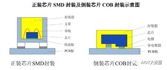
Detailed explanation of COB packaging process: the key to improving product quality
- author:
- 2024-05-27 10:56:26
Since the development of the LED display industry, a variety of production and packaging processes have emerged. At present, in the small-pitch market, SMT chip technology dominates; while in the micro-pitch market, COB packaging technology has gradually won the favor of the market due to its higher pixel density and more precise display effect. So, what steps are included in the COB packaging process?
01
What is COB packaging process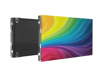
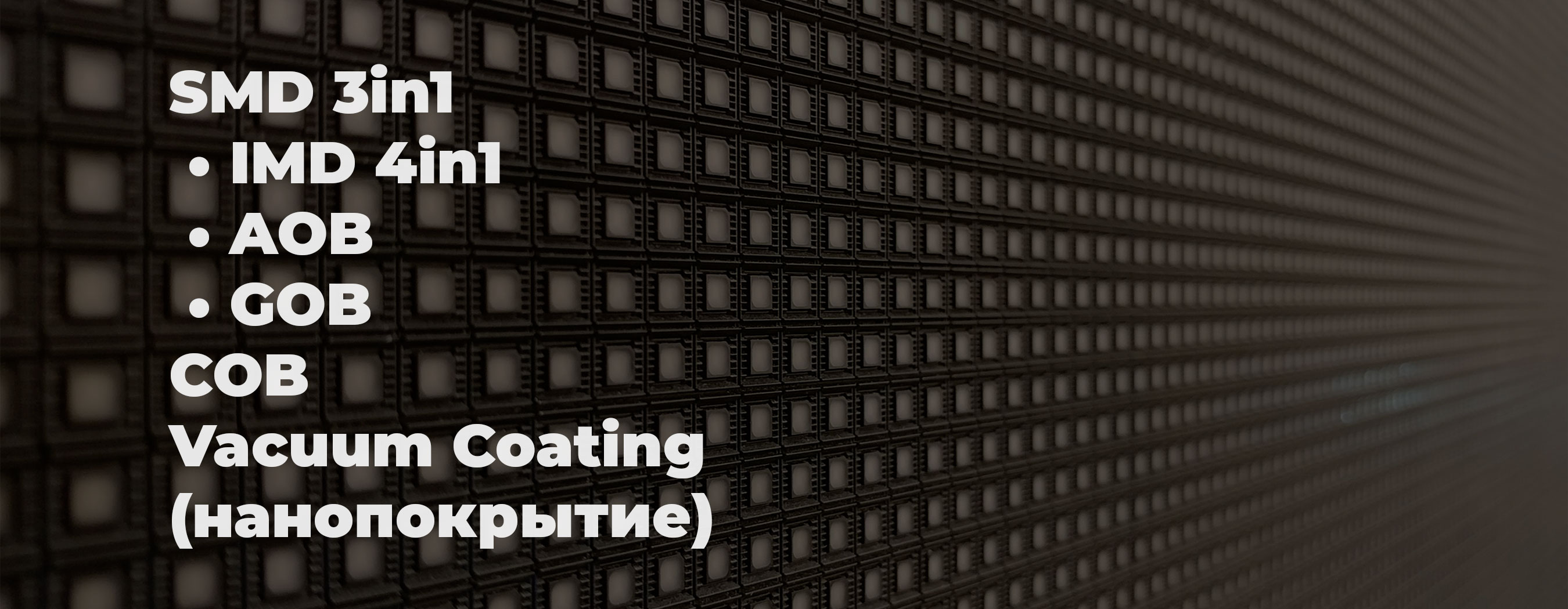
The COB packaging process, or Chip On Board packaging process, is a packaging method that directly mounts LED chips on a PCB. Compared with traditional SMD packaging methods, COB packaging has higher integration, stronger heat dissipation performance and more stable performance. At the same time, the COB packaging process also has the advantages of high production efficiency and low cost, so it has wide application prospects in the field of LED displays.
PART/01 Crystal expansion
Place the LED chip on the crystal expansion ring, and then place the crystal expansion ring on the adhesive surface where the silver paste layer has been scraped to perform the crystal expansion operation.
PART/02 Adhesive Adhesive
Place the expanded crystal expanding ring on an adhesive adhesive machine, and apply a suitable amount of silver paste on the PCB printed circuit board through a dispensing machine.
PART/03 Starring Crystal
Place the crystal expanding ring with prepared silver paste into the crystal piercing rack, and the operator uses a crystal piercing pen to stab the LED chip on the PCB printed circuit board under a microscope.
PART/04 Baking
Place the stung PCB printed circuit board into a thermal cycle oven and let it stand at a constant temperature for a period of time, and take it out after the silver paste is cured.
PART/05 Wafer
Use a dispenser to point an appropriate amount of red glue or vinyl onto the wafer position of the PCB printed circuit board, and then use anti-static equipment to accurately place the wafer on the red glue or vinyl.
PART/06 Coating
Use professional laminating equipment to cover the display with pre-prepared film material to protect and enhance the performance of the display.
PART/07 Curing
Put the sealed PCB printed circuit board into a thermal cycle oven and let it stand at a constant temperature. Different drying times can be set according to requirements.
PART/08 Post-test
Carry out the final inspection process to ensure that the quality of the COB display meets the requirements.
02
Advantages of COB packaging process
The COB packaging process supports multiple display modes and color adjustment functions, and can be personalized according to different application scenarios and needs to meet various display needs. Specifically, there are the following main points:
High brightness: COB packaging technology can directly mount LED chips on the PCB board, making the display brighter and clearer.
High contrast: COB packaging process can effectively improve the contrast of LED displays, making black deeper, white purer, and colors more vivid.
Long life: Because the COB packaging process has better heat dissipation performance and stability, the LED display has a longer life, reducing maintenance costs and replacement frequency.
Strong heat dissipation ability: COB products package LED light-emitting chips (wafers) on a PCB, and the heat from the wick is quickly transferred through the copper foil on the PCB. Moreover, the thickness of the copper foil on the PCB has strict process requirements., coupled with the gold sinking process, it will hardly cause serious light attenuation. Therefore, there are few dead lights, greatly extending the life of the lamp.
Wear resistant and easy to clean: The surface of the light spot is flat, smooth and hard, and is resistant to impact and wear; if defective spots occur, they can be repaired point by point; there is no mask, and dust can be cleaned with water or cloth.
Excellent all-weather characteristics: It adopts triple protective treatment, with outstanding waterproof, moisture, corrosion, dust, static electricity, oxidation and ultraviolet effects; it meets all-weather working conditions, and can still be used normally in an environment with a temperature difference of minus 20 degrees to 60 degrees above zero.
As an important innovation in the LED display industry, COB packaging technology brings better display effects and higher reliability to the micro-pitch market. By understanding its process flow, we can better understand the advantages and potential of this technology. With the continuous advancement of technology, COB packaging technology is expected to play a more important role in the future LED display market, bringing us a more exciting visual experience. Let us look forward to the further development and application of COB packaging technology, bringing new breakthroughs and changes to the LED display industry.
TAG:
Guess you want to see it
Popular information
-
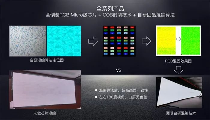
How to view the reasons for poor consistency of COB ink?

-
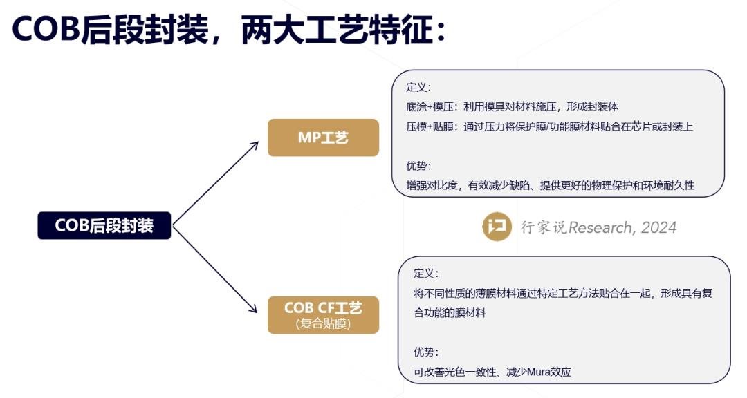
COB flushing, rear packaging attracts attention
-
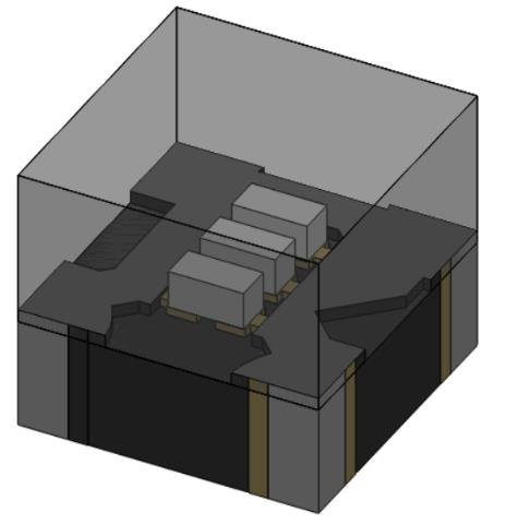
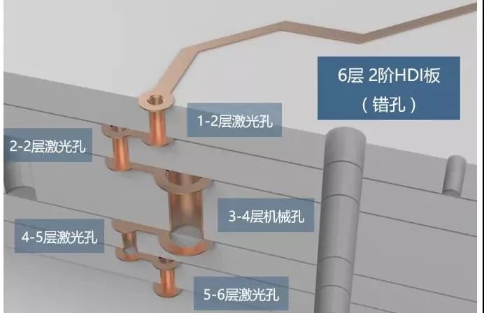
Analysis of COB mid-to-high-end PCB design process through 3D pictures
-
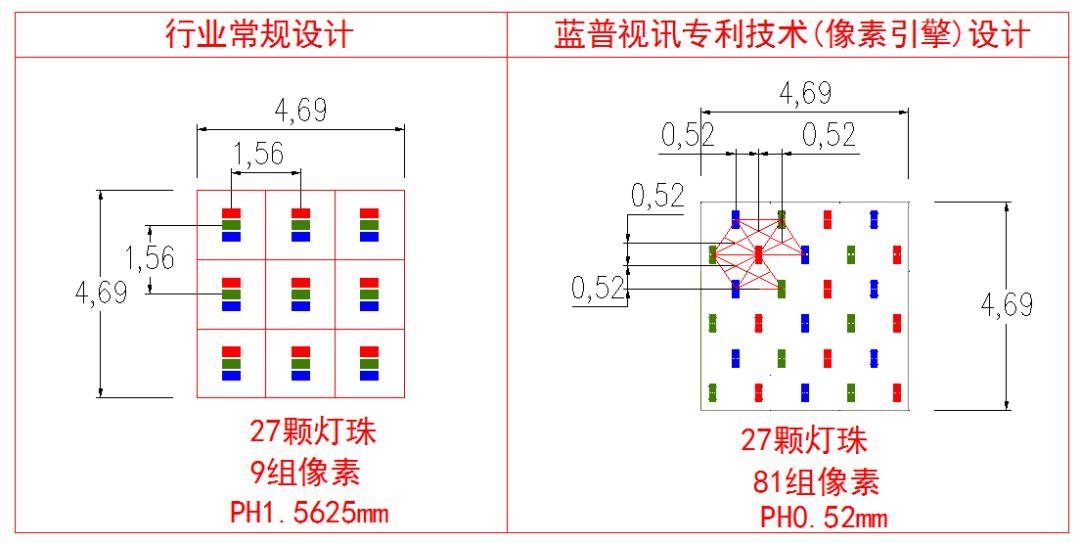
LED dynamic multiplexing pixel technology for COB and COG panels
-
Expand another 1100 COB production lines, and the MLED display card displays the "Big Era"
-
COB technology helps display enter the era of p0.XXmm HD
-
An article clearly understands what GOB is in led display protection technology, what are the advant
-
"Analysis of Key Points on COB Packaging Technology"
-
COB packaging: advantages and challenges coexist
-
What is the difference between GOB and COB displays?
the charts
- Technical analysis of COB, IMD, mini, micro LED market
- Expand another 1100 COB production lines, and the MLED display card displays the "Big Era"
- COB flushing, rear packaging attracts attention
- What is the difference between GOM,COB, and msd packages?
- Which of the two technologies is the mainstream route, MIP or COB?
- LED dynamic multiplexing pixel technology for COB and COG panels
- Detailed explanation of COB packaging process: the key to improving product quality
- Analyze outdoor COB display screens from Asian Games events
- Exploring the secret of LED screen production: Process comparison between COB technology and SMD tec
- What are the LED chip packaging materials used to package COBs?