Technical analysis of COB, IMD, mini, micro LED market
- author:
- 2023-02-23 09:19:52
In the past year, what is the hottest term in the LED direct display industry? It's not COB, IMD, mini LED or micro LED; it's MiP. MiP (Micro LED in Package), as a new packaging process for LED direct display suitable for new micro LED crystal particles, has been considered by many people in the industry to be the future P0.2-p3.0, LED direct display products, especially indoor high-performance direct display products. The standard answer.
MiP is making great strides and accelerating
In July 2022, Guoxing Optoelectronics announced the launch of a new MIP (Micro LED in Package) package device solution. The MIP display module has a high black ratio of over 99%, adopts a special optical design, and has a horizontal viewing angle of 174. It is compatible with current equipment machines. In 2022, two MIP glass-based packaging carrier boards from Vogel Optoelectronics were unveiled, 0404 and 0202 respectively. Among them, 0404 mainly corresponds to a 2*4mil RGB chip with a package size of 400*400um;0202 mainly corresponds to a 1*2mil RGB chip with a package size of 250*250um. At the end of 2022, San 'an Optoelectronics demonstrated the 0404 size MiP package device: the Micro LED chip used in this product has a size of 34*58um, the package size is 400*400um, the thickness is 150um, and the size of the four solder joints at the bottom of the device is 120um*120um...

In addition to the upstream market, in the end market, many companies including Sony, Liard, and Chuangxian Optoelectronics have also launched a large number of mass-produced MiP-packaged LED direct display products and deployed them as their respective flagship products and high-end products.
It can be said that MiP packaging will begin to emerge in 2021 and form a situation of upstream popularization in 2022; the industry expects that 2023 will be the first year of the explosion of MiP downstream products. More terminal brands will inevitably deploy MiP packaged products in 2023, especially terminal companies that do not have a huge transfer of technology. They can quickly enter the competitive track of micro LED direct display through MiP and create new high-quality flagship terminals for themselves. The latter will be MiP's biggest market attraction.
Necessary advantages of MiP packaging
It is a general trend for LED direct display technology to enter the micro LED era. There are two reasons: First, micro-pitch LED direct display products require smaller LED crystal particles, and micro LED is an inevitable basic requirement; second, with the advancement of LED technology and the improvement of luminous efficiency, smaller LED crystal particles can also meet the pixel brightness requirements, which is a low-cost and efficient choice for LED direct display.
At present, the micro LED upstream market has gathered tens of billions of investments. These investments will enter the production period around 2025. In the meantime, determining the midstream technical route of micro LEDs in direct display applications, that is, the packaging structure, has become an urgent task.
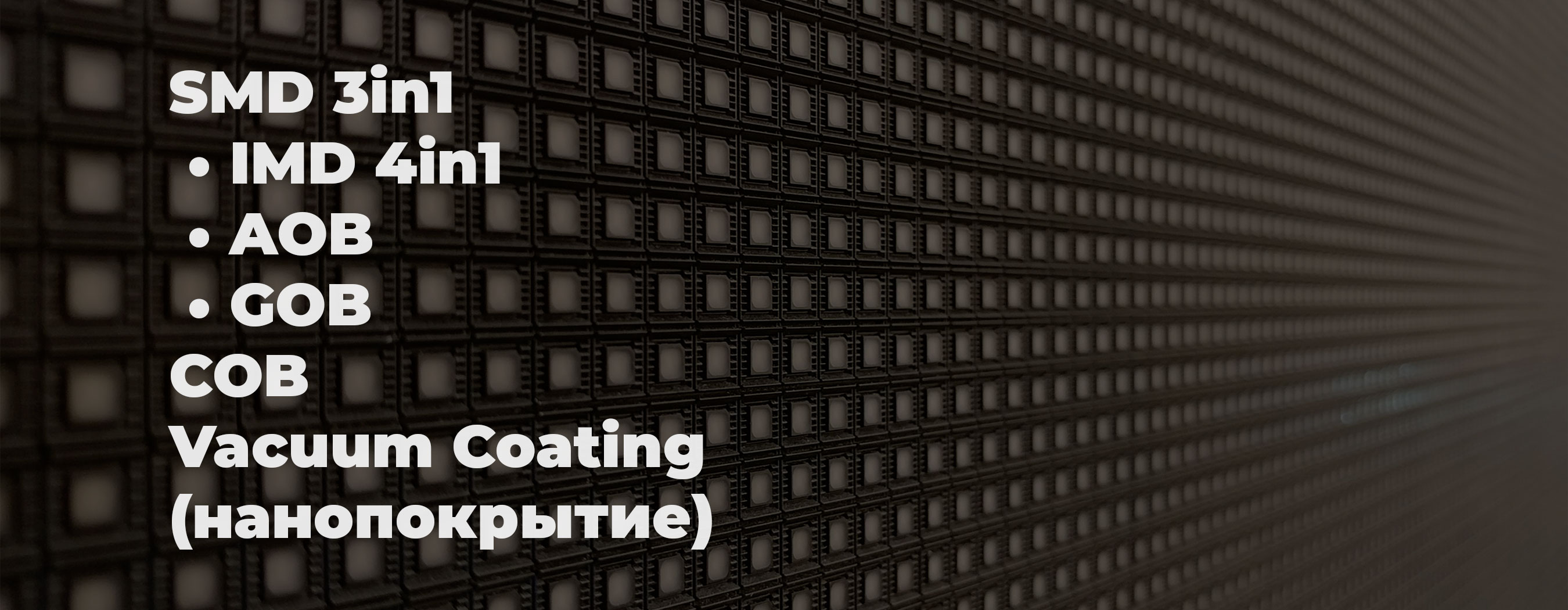
Compared with traditional packaging structures, such as COB, SMD and IMD, MiP has two major necessities in the micro LED era. One is that MiP is currently the most suitable package structure for smaller line widths. SMD can only package chips larger than 145um, IMD and COB can package chips with a size larger than 125um, and MiP can package the smallest size of LED chips, which can be below 60um. That is to say, MiP can make micro LED packaging, while COB, SMD and IMD can hardly, or reliability and economy are not allowed.

The second is that MiP is currently a more friendly technical route for direct display products to break through the huge transfer bottleneck in micro LED packaging. Huge transfer is the core process bottleneck of micro LED display. Among them, the biggest difficulty lies not in the huge amount, but in the huge amount of reliability: that is, most of the huge amount currently transfers to a yield rate of 4 9s, and a few leading companies have reached a yield rate of 6 9s.
For available display terminals, the yield rate of 6 9s is the basic threshold. That is, the 2K display does not have more than 4-6 bad dots. However, with MiP packaging, because it requires discrete device cutting and final packaging testing after massive transfers, the yield of massive transfers becomes an efficiency and cost issue rather than an unacceptable defect issue under the integrated package.
It can be said that from the perspective of the packaging process, MiP packaging has the efficiency of massive transfer and large batch processing, and the front-end processing process is highly large-scale and integrated; and it is cut into discrete devices through the back end, and there is no need to meet the requirements of direct integrated packaging. The extremely high yield rate provides advantages in terminal screen detection and repair.
That is, through MiP packaging technology, the industry can not only solve the problem of limit line width faced by micro LEDs, but also compromise problems such as huge transfer process difficulty and yield, testing, and repair. Solving these two problems will basically solve the core bottleneck of mass production applications of micro LEDs in the midstream packaging process.
MiP discrete devices are more friendly to downstream terminals"
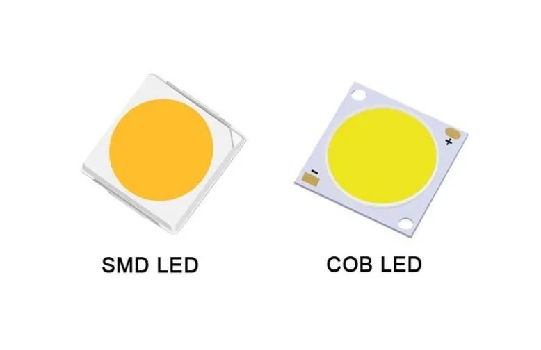
At present, the mainstream micro-pitch and small-pitch LED direct display packaging technologies are COB, SMD and IMD. Among them, the SMD packaging structure of the surface mount process cannot adapt well to mini LEDs and micro LEDs. Therefore, it can be said that only COB and IMD are the mainstream packaging structures that truly lead the continuous technological development and upgrading of LED direct display.
However, the emerging MiP is significantly different from COB and IMD. That is to say, COB and IMD are both integrated devices, while MiP focuses on discrete devices. As a discrete device, it has many terminal advantages:
First, Discrete devices have significant advantages in testing, debugging, consistency selection, and repair. Especially for MiP discrete devices, compared with the massive transfer technology under traditional integrated packaging, especially large-scale integrated packaging, it does not require LED particle testing on the micro LED wafer layer, but delays the testing phase to the packaging process. This will greatly help reduce the consistency and reliability threshold for micro LED upstream manufacturing and achieve better cost-friendliness.

And at the terminal level, MiP discrete devices are point-repairable. The difficulty of repairing integrated CELL that is not similar to COB. -- The scrapping losses of parts caused by defective dots vary greatly. This is conducive to reliability and quality cost control at the final product integration level.
Second, MiP discrete devices are a technology that is highly compatible with traditional discrete device terminal production lines. That is, the terminal production line of MiP discrete devices is basically the same as the SMD and IMD packaging structure. At the terminal stage, MiP has the advantages of high process connectivity and high degree of equipment use. It will reduce R & D and equipment investment. It will make MiP easier to popularize and be accepted by downstream companies in the market, especially by practitioners in small and medium-sized industries, and can quickly form a market. Scale advantage.
Third, MiP discrete devices have both the high reliability of COB integrated packages and the high consistency of SMD devices, and have excellent advantages in display performance. In fact, the industry generally believes that MiP technology is an ideal choice that integrates the advantages of COB, massive transfer, MID, SMD and other technologies, and balances and makes up for their respective disadvantages.
Fourth, MiP packaged products also have the advantage of versatility. In theory, a MiP of a package size can be compatible with the manufacturing of LED screen end products with a majority of dot spacing greater than that of the package size. This is different from the integrated packaging of COB and IMD. The packaging structure and midstream products directly determine the dot spacing of downstream products. That is, MiP has wider flexibility in terminal product design. This will also make MiP more popular among downstream manufacturers and reduce the density of midstream product specifications.
Overall, the advantages of MiP are reflected in all stages of the upper, middle and lower reaches. It has a higher degree of friendliness to the entire industry chain of micro LED direct display products. This is also the reason why this technical solution quickly became the direction of joint investment in the industry. Moreover, from the perspective of market competition, MiP also has better market cost friendliness.
TAG:
Guess you want to see it
Popular information
-
How to view the reasons for poor consistency of COB ink?

-
Three main development directions of COB packaging technology
-
What is the difference between GOB and COB displays?
-
An article clearly understands what GOB is in led display protection technology, what are the advant
-
The difference between COB package and traditional SMD package
-
Expand another 1100 COB production lines, and the MLED display card displays the "Big Era"
-
Technical analysis of COB, IMD, mini, micro LED market
-
2024 will directly show the rise of Mini COB's biggest dark horse
-
"Analysis of Key Points on COB Packaging Technology"
-
COB flushing, rear packaging attracts attention
the charts
- Technical analysis of COB, IMD, mini, micro LED market
- Expand another 1100 COB production lines, and the MLED display card displays the "Big Era"
- COB flushing, rear packaging attracts attention
- What is the difference between GOM,COB, and msd packages?
- Which of the two technologies is the mainstream route, MIP or COB?
- LED dynamic multiplexing pixel technology for COB and COG panels
- Detailed explanation of COB packaging process: the key to improving product quality
- Analyze outdoor COB display screens from Asian Games events
- Exploring the secret of LED screen production: Process comparison between COB technology and SMD tec
- What are the LED chip packaging materials used to package COBs?