Common comparisons between LED displays COB and GOB: Detailed explanation of advantages and disadvan
- author:
- 2024-05-27 11:24:57
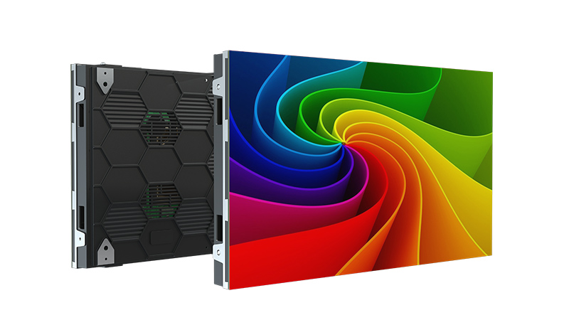
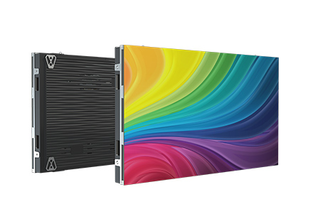
In today's era of rapid development of technology, various electronic products are emerging one after another. Among them, LED displays, as an important information display tool, are widely used in various fields. In the production process of LED displays, COB and GOB are two common technologies. GOB is a packaging technology that performs glue filling treatment based on SMD. It uses an advanced new transparent material to encapsulate the substrate and its LED packaging unit to form effective protection. This article will compare the two technologies in detail to help readers better understand the differences between them.
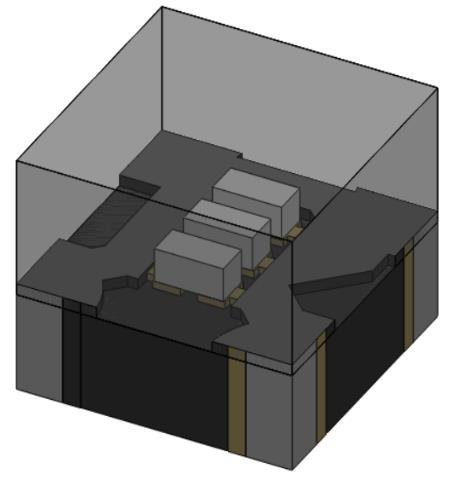
COB and GOB can be regarded as secondary sealing technologies for SMD products in terms of appearance, but there are big differences between the two in terms of materials and processes.
01
process advantages
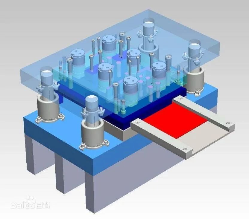
COB adopts a high-temperature pressing process, and GOB adopts a room-temperature dispensing process. COB is accurately controllable in terms of thermal stability, overall accuracy, flatness, and thickness. In particular, high-temperature pressing can solve the problem of glue cracking caused by heating and temperature rise in LED work.
COB adopts the same hot pressing forming process as COB, using high-precision tools for hot pressing. The colloid is pressed and formed in a molten state of 90%, and cured for 5-10 minutes.
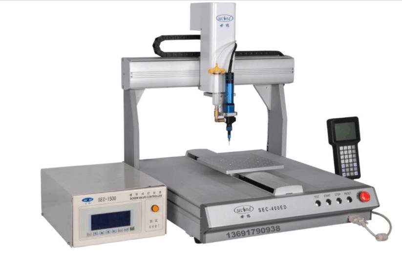
The ordinary epoxy resin solution adopted by GOB uses a fixture to allow the colloid to be automatically miscible and leveled at room temperature and then cured. Similar to the glue filling process of original outdoor products.
02
material advantages
COB refers to the COB process using high-temperature molded polymer synthetic colloid, which is added with various additives, coagulants, UV resistance, etc., which can solve the yellowing problem of ordinary epoxy. At the same time, through melanin adjustment and mold matte surface design.
03
Optical picture advantages
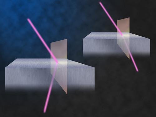
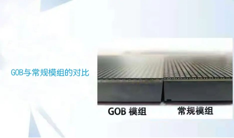
Due to the uncontrollable thickness of the finished product in the GOB process, and the difference in flatness of the self-leveling colloid, the finished product thickness of the GOB is generally relatively thick. Therefore, when splicing in large size, the problem of edge refraction is more obvious, which is commonly referred to as the problem of bright lines in the writing angle.
Because COB passes through precision mold tools, its thickness will only exceed the LED height by within 0.2mm at most, and light will hardly produce secondary refraction at the edge of the gel.
04
contrast advantage
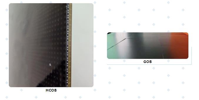
The finished surface of ordinary GOB process is a mirror surface, so it is impossible to achieve a matte surface or matte surface.
COB is formed with a matte surface through mold design and press molding, similar to a matte black lamp, and the contrast ratio of the entire screen is increased by 40%.
05
Accuracy advantages
COB adopts a high-precision mold process, and the overall forming accuracy can be controlled within 0.2mm according to the conventional mold accuracy. However, GOB's normal temperature forming is cured by internal condensation between molecules, which has a shrinkage problem. The current progress is preferably 0.5mm, and some require secondary processing. COB technology has been used in batches at mainstream pitches of 1.2, 1.5, and 1.8.
To sum up, COB and GOB are two different LED display packaging technologies, and they each have their own advantages and disadvantages. In practical applications, users should choose the appropriate packaging technology based on specific needs and budgets. With the continuous development of technology, COB and GOB technologies will continue to improve and innovate, bringing more possibilities to the LED display industry.
TAG:
Guess you want to see it
Popular information
-
What is the difference between GOB and COB displays?
-
Detailed explanation of COB packaging process: the key to improving product quality

-
COB packaging: advantages and challenges coexist
-
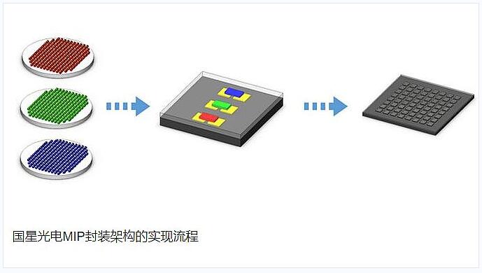
Which of the two technologies is the mainstream route, MIP or COB?
-
Exploring the secret of LED screen production: Process comparison between COB technology and SMD tec
-
Technical analysis of COB, IMD, mini, micro LED market
-
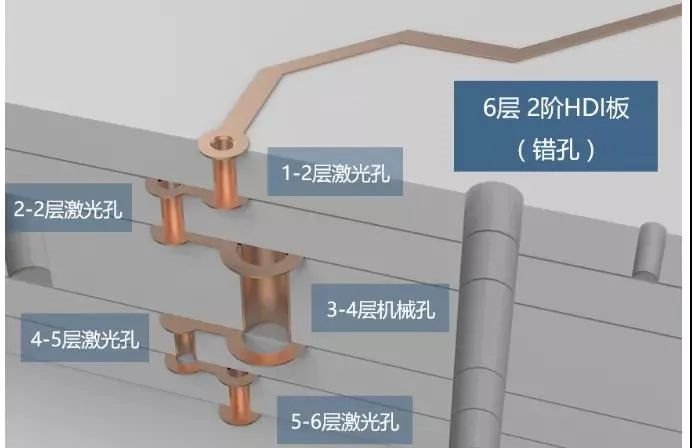
Analysis of COB mid-to-high-end PCB design process through 3D pictures
-
2024 will directly show the rise of Mini COB's biggest dark horse
-
"Analysis of Key Points on COB Packaging Technology"
-
The difference between COB package and traditional SMD package
the charts
- Technical analysis of COB, IMD, mini, micro LED market
- Expand another 1100 COB production lines, and the MLED display card displays the "Big Era"
- COB flushing, rear packaging attracts attention
- What is the difference between GOM,COB, and msd packages?
- Which of the two technologies is the mainstream route, MIP or COB?
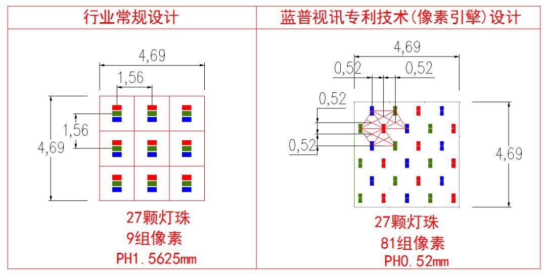
- LED dynamic multiplexing pixel technology for COB and COG panels
- Detailed explanation of COB packaging process: the key to improving product quality
- Analyze outdoor COB display screens from Asian Games events
- Exploring the secret of LED screen production: Process comparison between COB technology and SMD tec
- What are the LED chip packaging materials used to package COBs?