Analysis of COB mid-to-high-end PCB design process through 3D pictures
- author:
- 2024-05-27 11:39:33
In the field of modern electronic technology, the design process of PCB boards is crucial. As a key part of it, high-end PCB boards have many points worthy of in-depth exploration in their characteristics and manufacturing process.
High-end PCB, one of the key materials of COB, not only has an important impact on cost, but also has a great impact on the yield of the COB process. Today, several internal structural drawings of multi-layer PCB circuit boards were drawn, using three-dimensional graphics to show the internal structures of various PCB drawings with laminated structures.
01
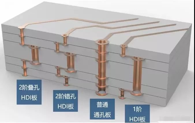
The core of high-density interconnection board (HDI) lies in vias.
In terms of circuit processing of multi-layer PCBs, it is not much different from single and double layers. The biggest difference is reflected in the via process. Lines are all made by etching, and vias are formed by drilling first and then copper plating. These are all known to those engaged in hardware development and will not go into detail here. Multi-layer circuit boards usually have several types: through-hole boards, first-stage boards, second-stage boards, and second-stage laminated hole boards. Higher-level boards such as three-level boards and arbitrary layer Internet boards are extremely rare in daily use and extremely expensive, so I won't discuss it too much for the time being.
Under normal circumstances, 8-bit MCU products use 2-layer through-hole boards;32-bit MCU level intelligent hardware will use 4-layer to 6-layer through-hole boards;Linux and Android level intelligent hardware will use 6-layer through-hole to 8-layer first-order HDI boards; compact products like smartphones usually use 8-layer first-order to 10-layer second-order circuit boards.

8-story and 2-step laminated holes, Qualcomm Xiaolong 624
02
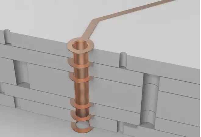
The most common through hole.
There is only one type of via, which runs from the first layer to the last layer. Whether it is an external line or an internal line, the holes are pierced through, which is called a through-hole plate. The via board has nothing to do with the number of layers. The 2 layers that everyone uses in ordinary times are basically via boards, while many switches and military circuit boards, even if they have 20 layers, are still via boards. The circuit board is drilled through with a drill bit, and then a copper plating operation is performed in the hole to form a via.
It should be noted here that the inner diameters of through holes are usually 0.2mm, 0.25mm and 0.3mm, but generally 0.2mm is much more expensive than 0.3mm. This is because the drill bit is too thin and easily breaks, and the drilling speed will be slightly slower. The extra time spent and the cost of the drill are reflected in the increase in circuit board prices.
03
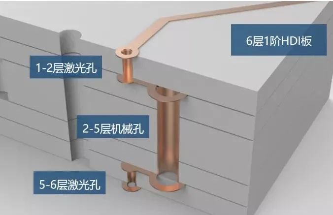
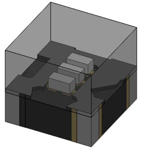
This picture is a laminated structure diagram of a 6-layer 1-level HDI board. Both surface layers are laser holes with an inner diameter of 0.1 mm. The inner layer is a mechanical hole, which is equivalent to a 4-layer through-hole plate, and the outside is covered with 2 layers. The laser can only penetrate glass fiber sheets, but cannot penetrate metal copper. Therefore, punching on the outer surface will not affect other internal lines. After laser drilling, copper plating is carried out to form laser vias.
04
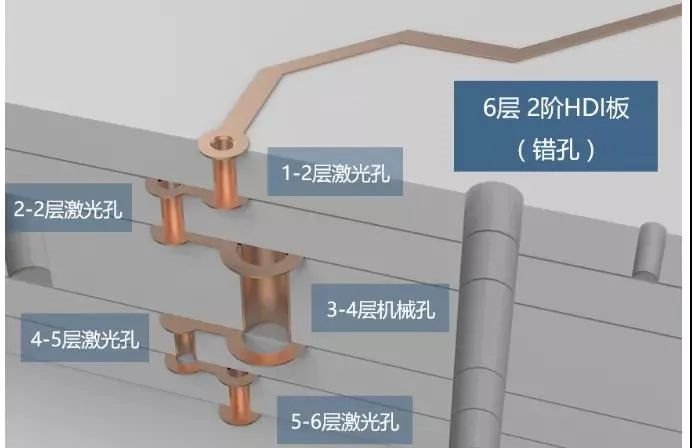
Two-layer laser holes on stage 2 HDI board
This picture is a 6-layer 2-stage staggered hole HDI board. Usually, there are fewer people using Level 6 and Level 2, and most of them start from Level 8 and Level 2. There are more floors here, which is the same as 6 floors. The so-called level 2 means that there are 2 layers of laser holes. The so-called staggered holes means that the two layers of laser holes are staggered. Then why staggered? This is because copper plating cannot be fully plated, and the hole is empty, so you cannot directly punch holes on it, you must stagger it a certain distance and make another layer of empty holes. 6 layers of second-level =4 layers of first-level plus 2 layers. 8 layers of second-level =6 layers of first-level plus 2 layers on the outside
Through a detailed analysis of the high-end PCB design process, we can have a deeper understanding of its key role in electronic equipment. It is hoped that these contents will provide valuable reference for research and practice in related fields and promote the continuous development of electronic technology.
TAG:
Guess you want to see it

Popular information
-
Analyze outdoor COB display screens from Asian Games events
-
COB technology helps display enter the era of p0.XXmm HD
-
Which of the two technologies is the mainstream route, MIP or COB?
-
Analysis of COB mid-to-high-end PCB design process through 3D pictures
-
An article clearly understands what GOB is in led display protection technology, what are the advant
-
Exploring the secret of LED screen production: Process comparison between COB technology and SMD tec
-
Detailed explanation of COB packaging process: the key to improving product quality

-
Common comparisons between LED displays COB and GOB: Detailed explanation of advantages and disadvan
-
Expand another 1100 COB production lines, and the MLED display card displays the "Big Era"

-
What are the LED chip packaging materials used to package COBs?
the charts
- Technical analysis of COB, IMD, mini, micro LED market
- Expand another 1100 COB production lines, and the MLED display card displays the "Big Era"
- COB flushing, rear packaging attracts attention
- What is the difference between GOM,COB, and msd packages?
- Which of the two technologies is the mainstream route, MIP or COB?
- LED dynamic multiplexing pixel technology for COB and COG panels
- Detailed explanation of COB packaging process: the key to improving product quality
- Analyze outdoor COB display screens from Asian Games events
- Exploring the secret of LED screen production: Process comparison between COB technology and SMD tec
- What are the LED chip packaging materials used to package COBs?