An article clearly understands what GOB is in led display protection technology, what are the advant
- author:
- 2024-09-03 16:59:46
The higher the resolution of an LED screen with a smaller physical screen size, the smaller the LEDs themselves and the distance between them. This leads to technical difficulties in placing, installing, and protecting LEDs during transportation and operation. This article is dedicated to analyzing existing technologies for protecting indoor LED screens from external influences.

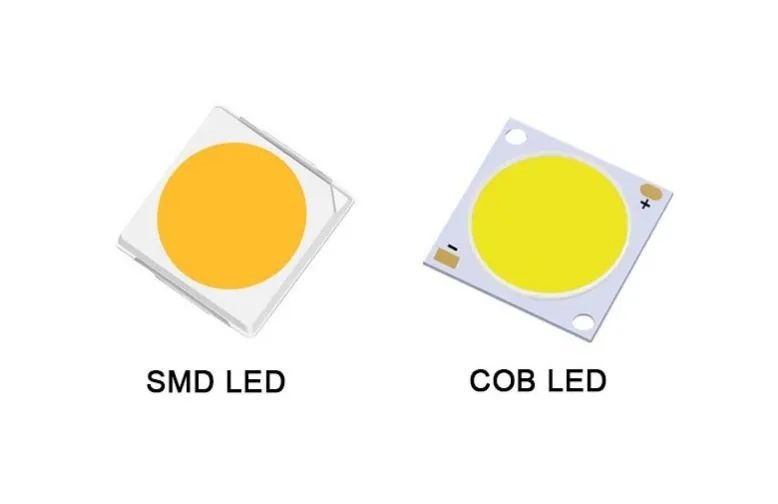
为了制造供室内使用的小像素间距 LED 屏幕,采用了 SMD3in1 表面贴装技术。Recently we have been discussing using COB technology to grow LEDs directly on the board. SMD3in1 surface mount technology has been widely used due to its balanced technical characteristics-color uniformity, saturation, viewing angle, power consumption, convenient maintenance methods, etc. Although COB has many advantages, it also has enough shortcomings, which makes mass production difficult, so the era of LED large-screen technologies using the technology of growing crystals directly on the board has not yet arrived.
由于制造商每年都在缩小像素间距,以更小的物理屏幕尺寸实现更高的分辨率,因此出现了许多与屏幕过热有关的问题,这意味着LED烧毁,LED在运输过程中因焊盘过小而脱落以及安装、接触氧化、潮湿、灰尘等问题。
因此,需要对屏幕进行一些保护,以延长 LED 本身以及组件在运输和操作过程中的使用寿命,尤其是在像素间距较小的情况下。On the other hand, protective coatings must be used in certain areas to provide small but vandal-proof protection.
总之,有几个方面可以保护免受外部物理影响。This article will discuss the main technical methods to change technical characteristics by applying special protective layers or changing production techniques and fixing the LEDs to a printed circuit board.

95% of LED screens are produced based on mature technology.
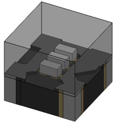
放置在白色/黑色塑料或陶瓷外壳中的 SMD LED 的结构具有以下横截面图。

考虑到直到最近几乎所有屏幕都使用这种技术生产的事实,它既有优点也有一些缺点。
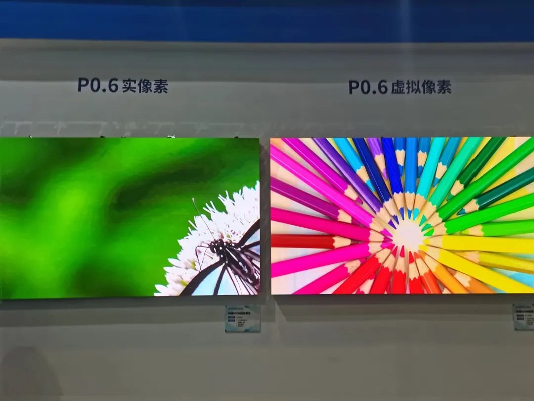
但由于 SMD 技术可以让您创建颜色均匀度均匀的屏幕,在功耗、亮度、颜色饱和度方面具有平衡的特性,并且能够创建间距小于 1 毫米的屏幕:0.6-0.9 毫米 - 制造商正在开发各种方法保护这些屏幕免受外部影响并延长 LED 的"寿命"。
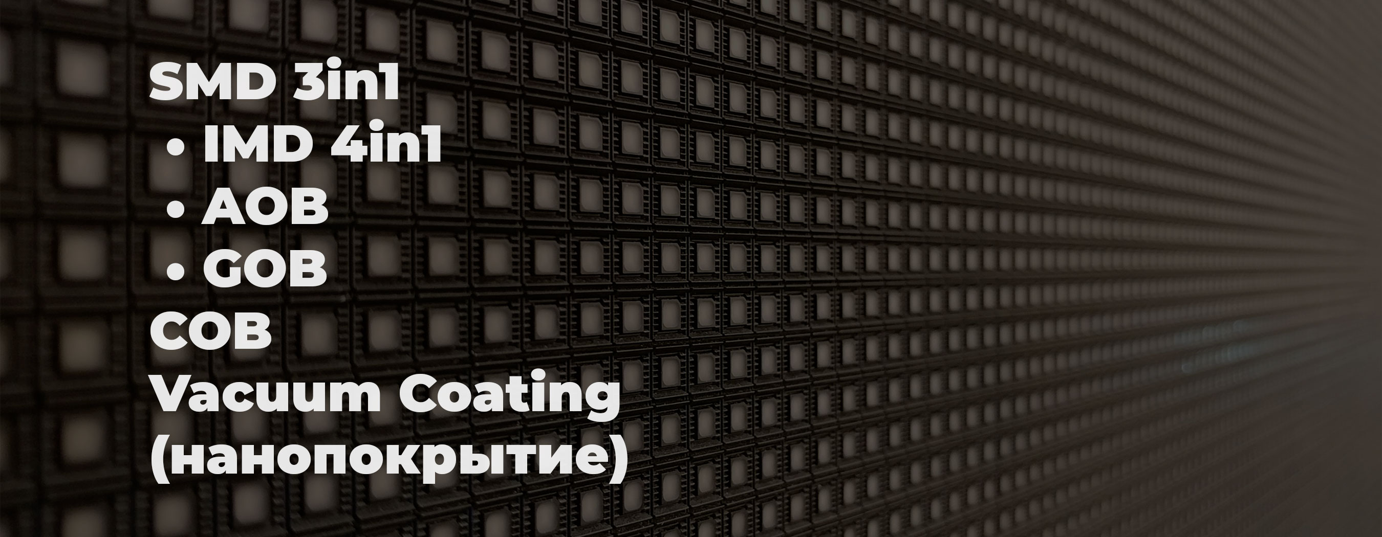
因此,如今用于室内空间的 LED(LED 屏幕)生产有两种主要技术:SMD3in1 和越来越多的 COB。The SMD3in1 has IMD4in1 design options and also has special compound coatings- AOB and GOB technologies. In addition, LED display modules in production can be coated with nano coatings-vacuum coating.

这项技术通常也被称为 mini-LED,在之前的文章 中也详细介绍过。It allows you to use a set of 4 SMD3in1 LEDs to protect the LED screen while adding solder pads to increase the adhesion of the LEDs in the printed circuit board area and simplify maintenance of the LED module.
一个区域为4个像素,步长由平均值决定。Due to the different distance between the LEDs on one site and adjacent sites. The difference is small, but it does exist.
SMD的标准"焊接强度"约为每撕裂1-1.5公斤,IMD 4in1将这一数字增加至约4.5公斤。

重要的一点是,LED 的表面是"粗糙、哑光"的,而不是"镜面状"的;这是专门为了保护屏幕免受光线再反射并实现高对比度而设计的。
These technologies are based on the addition of special adhesives to protect LED strips.
This technology only fills the legs of the LED, the leads, with a special adhesive composition"". Therefore, filling technology can improve protection against contact oxidation and can also improve the adhesion coefficient between the diode and the circuit board. Then cover it with a transparent protective layer. The protective layer is a polymer material applied using nanotechnology (similar to vacuum coating).
使用 SMD 技术组装的屏幕还可以获得防潮保护,以及屏幕在运输和安装过程中可能受到的轻微损坏和划痕。
该技术具有以下结构。

The result is a fairly strong structure with the following characteristics.

这种技术让人想起COB,仅使用SMD表面贴装技术来制造LED,将LED放置在板上后,模块本身涂上特殊的粘合剂组合物,然后再涂上透明保护层。
涂层技术与AOB类似,但这种情况下整个表面都覆盖有保护层,如下图所示。


以这种方式涂覆的模块 - 带有粘合剂和保护性透明层,采用 AOB 和 GOB 技术,增强了屏幕免受机械损坏、湿气和灰尘的保护。This protection does not mean that screens can be used outdoors, they are only used indoors.
总结GOB技术,我们得到以下特点。
相比之下,这两种技术如下所示:

The technology known as" vacuum coating" is a process that uses vacuum technology to create a pressurized environment (subatmospheric pressure) to coat films and coatings by depositing an atomic or molecular source of condensable vapor (gas).
该技术可与任何LED屏幕技术结合使用,不仅为二极管提供保护,还为电子元件提供保护。
所使用的涂层源可以由各种不同的材料制成,从金属到氧化物和化合物,每种材料都具有不同的特性。For example, the films applied can be chemically resistant to corrosion and scratch, have high thermal conductivity and resistivity, which together protect and extend the life of the LED itself and the microelectronic device. This coating is invisible to the human eye, but at the same time protects the components of the microcircuit.
The previous article mainly introduced COB technology. In short, this technology should replace the widely used SMD3in1 and IMD4in1 surface mount technologies in the future. It has multiple options for creating LEDs-but they all boil down to growing the diodes directly on the board. Scientists say the technology will completely eliminate contacts made of gold (currently, alloys of gold or other metals are used; gold adds several times to the overall cost of LEDs and screens compared to alloys using other metals)
为了制造供室内使用的小像素间距 LED 屏幕,采用了 SMD3in1 表面贴装技术。Recently we have been discussing using COB technology to grow LEDs directly on the board. SMD3in1 surface mount technology has been widely used due to its balanced technical characteristics-color uniformity, saturation, viewing angle, power consumption, convenient maintenance methods, etc. Although COB has many advantages, it also has enough shortcomings, which makes mass production difficult, so the era of LED large-screen technologies using the technology of growing crystals directly on the board has not yet arrived.
由于制造商每年都在缩小像素间距,以更小的物理屏幕尺寸实现更高的分辨率,因此出现了许多与屏幕过热有关的问题,这意味着LED烧毁,LED在运输过程中因焊盘过小而脱落以及安装、接触氧化、潮湿、灰尘等问题。
因此,需要对屏幕进行一些保护,以延长 LED 本身以及组件在运输和操作过程中的使用寿命,尤其是在像素间距较小的情况下。On the other hand, protective coatings must be used in certain areas to provide small but vandal-proof protection.
总之,有几个方面可以保护免受外部物理影响。This article will discuss the main technical methods to change technical characteristics by applying special protective layers or changing production techniques and fixing the LEDs to a printed circuit board.

SMD– surface mount device
95% of LED screens are produced based on mature technology.
放置在白色/黑色塑料或陶瓷外壳中的 SMD LED 的结构具有以下横截面图。

考虑到直到最近几乎所有屏幕都使用这种技术生产的事实,它既有优点也有一些缺点。
| advantages | disadvantages |
|---|---|
|
|
但由于 SMD 技术可以让您创建颜色均匀度均匀的屏幕,在功耗、亮度、颜色饱和度方面具有平衡的特性,并且能够创建间距小于 1 毫米的屏幕:0.6-0.9 毫米 - 制造商正在开发各种方法保护这些屏幕免受外部影响并延长 LED 的"寿命"。
因此,如今用于室内空间的 LED(LED 屏幕)生产有两种主要技术:SMD3in1 和越来越多的 COB。The SMD3in1 has IMD4in1 design options and also has special compound coatings- AOB and GOB technologies. In addition, LED display modules in production can be coated with nano coatings-vacuum coating.
IMD 4 in 1

这项技术通常也被称为 mini-LED,在之前的文章 中也详细介绍过。It allows you to use a set of 4 SMD3in1 LEDs to protect the LED screen while adding solder pads to increase the adhesion of the LEDs in the printed circuit board area and simplify maintenance of the LED module.
一个区域为4个像素,步长由平均值决定。Due to the different distance between the LEDs on one site and adjacent sites. The difference is small, but it does exist.
SMD的标准"焊接强度"约为每撕裂1-1.5公斤,IMD 4in1将这一数字增加至约4.5公斤。

重要的一点是,LED 的表面是"粗糙、哑光"的,而不是"镜面状"的;这是专门为了保护屏幕免受光线再反射并实现高对比度而设计的。
AOB and GOB technology
These technologies are based on the addition of special adhesives to protect LED strips.
AOB-on-board adhesive
This technology only fills the legs of the LED, the leads, with a special adhesive composition"". Therefore, filling technology can improve protection against contact oxidation and can also improve the adhesion coefficient between the diode and the circuit board. Then cover it with a transparent protective layer. The protective layer is a polymer material applied using nanotechnology (similar to vacuum coating).
使用 SMD 技术组装的屏幕还可以获得防潮保护,以及屏幕在运输和安装过程中可能受到的轻微损坏和划痕。
该技术具有以下结构。

The result is a fairly strong structure with the following characteristics.
| advantages | disadvantages |
|---|---|
|
|
GOB– board gluing

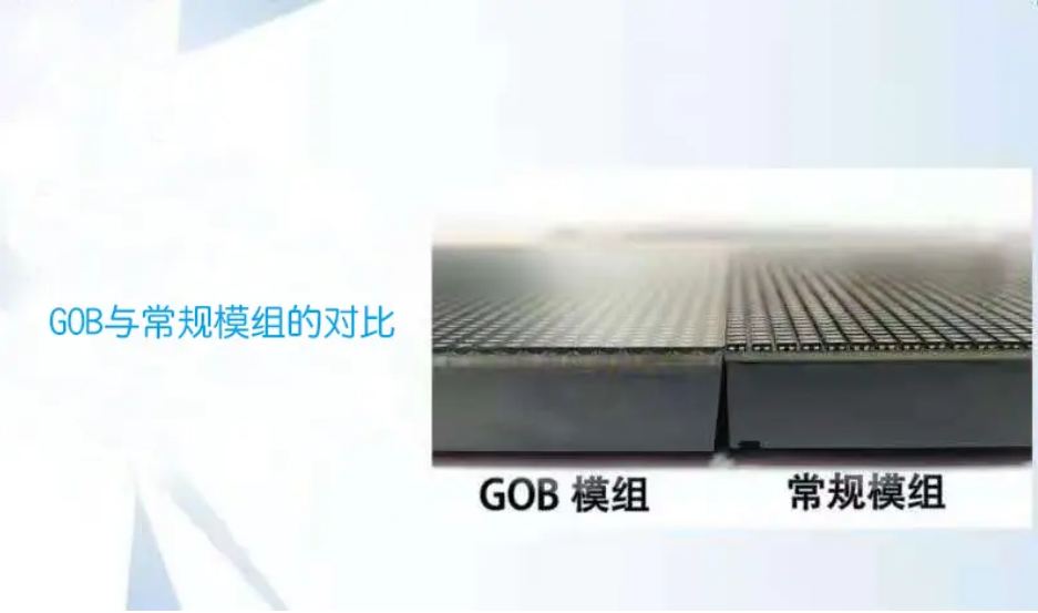
这种技术让人想起COB,仅使用SMD表面贴装技术来制造LED,将LED放置在板上后,模块本身涂上特殊的粘合剂组合物,然后再涂上透明保护层。
涂层技术与AOB类似,但这种情况下整个表面都覆盖有保护层,如下图所示。

PS According" to the name Glue on-Board", the space between the LEDs is filled with some kind of adhesive composition. Almost all sources on the Internet say that GOB is built in a similar way to AOB, except that the protective layer fills the entire space between the LEDs to make the surface smooth, while AOB only covers the legs. After understanding these technologies and communicating with manufacturer representatives, we can conclude that GOB is not coated with an adhesive component (such as AOB), but is coated with an epoxy resin (commonly called a compound) and then coated with a transparent protective layer using nanotechnology.

以这种方式涂覆的模块 - 带有粘合剂和保护性透明层,采用 AOB 和 GOB 技术,增强了屏幕免受机械损坏、湿气和灰尘的保护。This protection does not mean that screens can be used outdoors, they are only used indoors.
总结GOB技术,我们得到以下特点。
| advantages | disadvantages |
|---|---|
|
|
相比之下,这两种技术如下所示:

Nanocoating or special mask
The technology known as" vacuum coating" is a process that uses vacuum technology to create a pressurized environment (subatmospheric pressure) to coat films and coatings by depositing an atomic or molecular source of condensable vapor (gas).
该技术可与任何LED屏幕技术结合使用,不仅为二极管提供保护,还为电子元件提供保护。
所使用的涂层源可以由各种不同的材料制成,从金属到氧化物和化合物,每种材料都具有不同的特性。For example, the films applied can be chemically resistant to corrosion and scratch, have high thermal conductivity and resistivity, which together protect and extend the life of the LED itself and the microelectronic device. This coating is invisible to the human eye, but at the same time protects the components of the microcircuit.
COB
The previous article mainly introduced COB technology. In short, this technology should replace the widely used SMD3in1 and IMD4in1 surface mount technologies in the future. It has multiple options for creating LEDs-but they all boil down to growing the diodes directly on the board. Scientists say the technology will completely eliminate contacts made of gold (currently, alloys of gold or other metals are used; gold adds several times to the overall cost of LEDs and screens compared to alloys using other metals)
TAG:
Guess you want to see it
Popular information
-
Analyze outdoor COB display screens from Asian Games events
-
LED dynamic multiplexing pixel technology for COB and COG panels
-
Technical analysis of COB, IMD, mini, micro LED market
-
COB packaging: advantages and challenges coexist
-
Detailed explanation of COB packaging process: the key to improving product quality

-
What is the difference between GOM,COB, and msd packages?
-
The difference between COB package and traditional SMD package
-
Exploring the secret of LED screen production: Process comparison between COB technology and SMD tec
-
2024 will directly show the rise of Mini COB's biggest dark horse
-
How to view the reasons for poor consistency of COB ink?
the charts
- Technical analysis of COB, IMD, mini, micro LED market
- Expand another 1100 COB production lines, and the MLED display card displays the "Big Era"
- COB flushing, rear packaging attracts attention
- What is the difference between GOM,COB, and msd packages?
- Which of the two technologies is the mainstream route, MIP or COB?
- LED dynamic multiplexing pixel technology for COB and COG panels
- Detailed explanation of COB packaging process: the key to improving product quality
- Analyze outdoor COB display screens from Asian Games events
- Exploring the secret of LED screen production: Process comparison between COB technology and SMD tec
- What are the LED chip packaging materials used to package COBs?