In-depth analysis of LED packaging technology: ceramic COB technology
- author:
- 2024-05-27 17:01:16
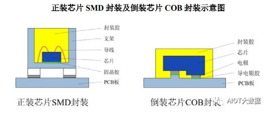
LED packaging technology is mainly divided into lens type and reflective cup type. Lens forming can be molded or lens bonded, while reflective cup type chips are formed by glue mixing, dispensing, and packaging. In recent years, with the gradual maturity of epitaxial, die bonding and packaging designs, the size and structure of LED chips have become increasingly miniaturized, and the power of a high-power single chip can reach 1- 3W or even higher, which has a high impact on LED chip carrier boards and system circuit boards. Higher requirements have been put forward for heat dissipation and heat resistance. In order to meet comprehensive properties such as insulation, withstand voltage, heat dissipation and heat resistance, ceramic substrates have become one of the important materials in chip sub-adhesion technology.
Ceramic substrate technology can be divided into thick film process, low temperature co-firing process and thin film process. However, thick film process and low temperature co-firing process using screen printing technology and high temperature sintering, easy to appear line rough, alignment is not accurate and shrinkage ratio problems, for fine lines of high-power LED products or requirements for accurate alignment of eutectic/flip chip process LED products, thick film and low temperature co-fired ceramic substrates have gradually failed to meet the demand.
The high heat dissipation coefficient thin film ceramic heat dissipation substrate is made by sputtering, electro/chemical deposition and yellow lithography processes. It has the characteristics of accurate metal lines and stable material systems. It is suitable for high-power, small size, and high-brightness LED development trends, especially solves the strict requirements of eutectic/flip chip packaging technology on the resolution and accuracy of metal lines on ceramic substrates. When the LED chip uses ceramics as the carrier, the cooling bottleneck of the LED module is transferred to the system circuit board, which transfers heat energy from the LED chip to the cooling fins and the atmosphere. With the continuous improvement of the functions of LED chips, materials have gradually changed from FR4 to metal-core printed circuit boards. However, the demand for high-power LEDs has made the heat dissipation coefficient of MCPCB materials unable to meet the requirements, so the demand for ceramic circuit boards has gradually become popular. In order to ensure the material stability and light attenuation stability of LED products under high-power operation, the trend of using ceramics as heat dissipation and metal wiring substrates is becoming increasingly obvious. At present, the cost of ceramic materials is higher than that of MCPCB. Therefore, while taking advantage of the high heat dissipation coefficient of ceramics, how to save material area to reduce production costs has become one of the important indicators for the development of ceramic LEDs. In recent years, the integration of polycrystalline packages and system circuits using ceramic COB designs has gradually attracted the attention of various package and system manufacturers.
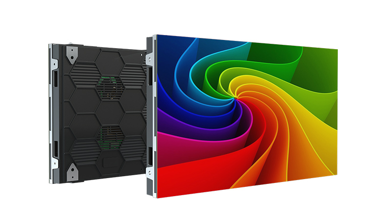
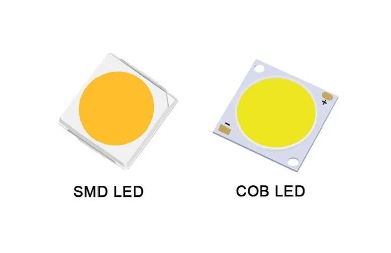
COB is not a new technology in the electronics manufacturing industry. It refers to directly pasting the bare epitaxial wafer on the circuit board, and directly soldering the wires/bonding wires on the gold-plated lines of the PCB. It is also called wire bonding, and then passing Sealing technology transfers the packaging steps in the IC manufacturing process to the circuit board for direct assembly. In the LED industry, due to the pursuit of lightness and high portability of modern technology products, and in order to save system board space for multiple LED chips, COB technology that directly attaches chips to the system board has been developed in the demand for high-power LED systems.
The advantages of COB include high cost-effectiveness, simple circuit design, saving system board space, etc., but there are also technical thresholds for chip integration brightness, color temperature harmony and system integration. Taking a 25W LED as an example, a traditional high-power 25W LED light source requires 25 1W LED chips to be packaged into 25 LED elements, while a COB package packages 25 1W LED chips into a single chip. Therefore, the number of secondary optical lenses required will be reduced from 25 to 1, which will help reduce the light source area, reduce material and system costs. This further simplifies the secondary optical design of the light source system and saves assembly labor costs. In addition, the high-power COB package only requires a single high-power LED to replace multiple LED packages of more than 1 watt (inclusive), making the product lighter and shorter.
At present, the production of COB products on the market still mainly uses MCPCB substrates. However, MCPCB still has problems such as heat dissipation and excessive light source area that need to be solved. Therefore, starting from updating the heat dissipation material is the most effective solution. Ceramic COB substrates have the following advantages: 1. Thin film technology makes the basic circuit more accurate;2. Large quantity reduces costs;3. High plasticity and can be designed according to different needs.
Existing LED bulbs made of MCPCB substrates and COB chips cannot be dimmed. However, LED dimmable bulbs assembled by ledaladdin Company using ceramic COB chips have been launched. They are available in specifications such as 5W, 6W, and 7W, with better performance and color temperature. It can reach 2200K-8000K, and the flow rate can reach more than 60LM/W.
The development of ceramic MCOB/COB is a trend to simplify system boards. The practicality, brightness, heat dissipation and cost control of lighting fixtures are all important key factors.
Ceramic substrate technology can be divided into thick film process, low temperature co-firing process and thin film process. However, thick film process and low temperature co-firing process using screen printing technology and high temperature sintering, easy to appear line rough, alignment is not accurate and shrinkage ratio problems, for fine lines of high-power LED products or requirements for accurate alignment of eutectic/flip chip process LED products, thick film and low temperature co-fired ceramic substrates have gradually failed to meet the demand.
The high heat dissipation coefficient thin film ceramic heat dissipation substrate is made by sputtering, electro/chemical deposition and yellow lithography processes. It has the characteristics of accurate metal lines and stable material systems. It is suitable for high-power, small size, and high-brightness LED development trends, especially solves the strict requirements of eutectic/flip chip packaging technology on the resolution and accuracy of metal lines on ceramic substrates. When the LED chip uses ceramics as the carrier, the cooling bottleneck of the LED module is transferred to the system circuit board, which transfers heat energy from the LED chip to the cooling fins and the atmosphere. With the continuous improvement of the functions of LED chips, materials have gradually changed from FR4 to metal-core printed circuit boards. However, the demand for high-power LEDs has made the heat dissipation coefficient of MCPCB materials unable to meet the requirements, so the demand for ceramic circuit boards has gradually become popular. In order to ensure the material stability and light attenuation stability of LED products under high-power operation, the trend of using ceramics as heat dissipation and metal wiring substrates is becoming increasingly obvious. At present, the cost of ceramic materials is higher than that of MCPCB. Therefore, while taking advantage of the high heat dissipation coefficient of ceramics, how to save material area to reduce production costs has become one of the important indicators for the development of ceramic LEDs. In recent years, the integration of polycrystalline packages and system circuits using ceramic COB designs has gradually attracted the attention of various package and system manufacturers.
COB is not a new technology in the electronics manufacturing industry. It refers to directly pasting the bare epitaxial wafer on the circuit board, and directly soldering the wires/bonding wires on the gold-plated lines of the PCB. It is also called wire bonding, and then passing Sealing technology transfers the packaging steps in the IC manufacturing process to the circuit board for direct assembly. In the LED industry, due to the pursuit of lightness and high portability of modern technology products, and in order to save system board space for multiple LED chips, COB technology that directly attaches chips to the system board has been developed in the demand for high-power LED systems.
The advantages of COB include high cost-effectiveness, simple circuit design, saving system board space, etc., but there are also technical thresholds for chip integration brightness, color temperature harmony and system integration. Taking a 25W LED as an example, a traditional high-power 25W LED light source requires 25 1W LED chips to be packaged into 25 LED elements, while a COB package packages 25 1W LED chips into a single chip. Therefore, the number of secondary optical lenses required will be reduced from 25 to 1, which will help reduce the light source area, reduce material and system costs. This further simplifies the secondary optical design of the light source system and saves assembly labor costs. In addition, the high-power COB package only requires a single high-power LED to replace multiple LED packages of more than 1 watt (inclusive), making the product lighter and shorter.
At present, the production of COB products on the market still mainly uses MCPCB substrates. However, MCPCB still has problems such as heat dissipation and excessive light source area that need to be solved. Therefore, starting from updating the heat dissipation material is the most effective solution. Ceramic COB substrates have the following advantages: 1. Thin film technology makes the basic circuit more accurate;2. Large quantity reduces costs;3. High plasticity and can be designed according to different needs.
Existing LED bulbs made of MCPCB substrates and COB chips cannot be dimmed. However, LED dimmable bulbs assembled by ledaladdin Company using ceramic COB chips have been launched. They are available in specifications such as 5W, 6W, and 7W, with better performance and color temperature. It can reach 2200K-8000K, and the flow rate can reach more than 60LM/W.
The development of ceramic MCOB/COB is a trend to simplify system boards. The practicality, brightness, heat dissipation and cost control of lighting fixtures are all important key factors.
TAG:
Guess you want to see it
Popular information
-
LED dynamic multiplexing pixel technology for COB and COG panels
-
Technical analysis of COB, IMD, mini, micro LED market
-
Which of the two technologies is the mainstream route, MIP or COB?
-
How to view the reasons for poor consistency of COB ink?
-
2024 will directly show the rise of Mini COB's biggest dark horse
-
COB technology helps display enter the era of p0.XXmm HD
-
What is the difference between GOM,COB, and msd packages?
-
An article clearly understands what GOB is in led display protection technology, what are the advant
-
What is the difference between GOB and COB displays?
-
Analyze outdoor COB display screens from Asian Games events
the charts
- Technical analysis of COB, IMD, mini, micro LED market
- Expand another 1100 COB production lines, and the MLED display card displays the "Big Era"
- COB flushing, rear packaging attracts attention
- What is the difference between GOM,COB, and msd packages?
- Which of the two technologies is the mainstream route, MIP or COB?
- LED dynamic multiplexing pixel technology for COB and COG panels
- Detailed explanation of COB packaging process: the key to improving product quality
- Analyze outdoor COB display screens from Asian Games events
- Exploring the secret of LED screen production: Process comparison between COB technology and SMD tec
- What are the LED chip packaging materials used to package COBs?